13
Electrical Specifications, Isolated Modulator
Unless otherwise noted, all specifications are at V
= 0 V and V = 0 V, all Typical specifications are at
IN+
IN-
T = 25°C and V
= V
= 5 V, and all Minimum and Maximum specifications apply over the following
A
DD1
DD2
ranges: T = -40°C to +85°C, V
= 4.5 to 5.5 V and V
= 4.5 to 5.5 V.
A
DD1
DD2
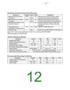
Parameter
Symbol Min. Typ. Max. Units
Test Conditions
Fig. Note
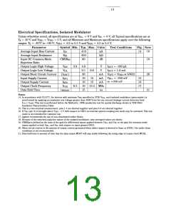
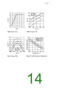
Average Input Bias Current
Average Input Resistance
Input DC Common-Mode
Rejection Ratio
I
R
-0.8
450
60
µA
kΩ
dB
14
18
IN
IN
CMRR
19
IN
Output Logic High Voltage
Output Logic Low Voltage
Output Short Circuit Current
Input Supply Current
Output Supply Current
Output Clock Frequency
Data Hold Time
V
3.9
8.2
4.9
0.1
30
10
V
V
mA
mA
mA
I
I
V
= -100 µA
= 1.6 mA
= V or GND2
DD2
= -350 mV
OH
OUT
OUT
V
0.6
OL
|I
I
I
|
20
21
OSC
DD1
DD2
CLK
OUT
15
15
V
15
16
17
IN+
to +350 mV
10
f
10 13.2 MHz
15 ns
t
HDDAT
Notes:
14. In accordance with UL1577, for devices with minimum V
specified at 3750 V , each isolated modulator (optocoupler) is
rms
ISO
proof-tested by applying an insulation test voltage greater than 4500 Vrms for one second (leakage current detection limit
I - < 5 µa). This test is performed before the Method b, 100% production test for partial discharge shown in VDE 0884
I O
Insulation Characteristics Table.
15. This is a two-terminal measurement: pins 1-4 are shorted together and pins 5-8 are shorted together.
16. If V (pin 3) is brought above V
- 2 V with respect to GND1 an internal optical-coupling test mode may be activated. This test
IN-
DD1
mode is not intended for customer use.
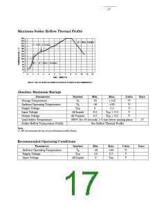
17. Agilent recommends the use of non-chlorinated solder fluxes.
18. Because of the switched-capacitor nature of the isolated modulator, time averaged values are shown.
19. CMRR is defined as the ratio of the gain for differential inputs applied between V
and V to the gain for common-mode
IN
IN+
IN-
inputs applied to both V
and V with respect to input ground GND1.
IN+
IN-
20. Short-circuit current is the amount of output current generated when either output is shorted to V
conditions is not recommended.
or GND2. Use under these
DD2
21. Data hold time is amount of time that the data output MDAT will stay stable following the rising edge of output clock MCLK.

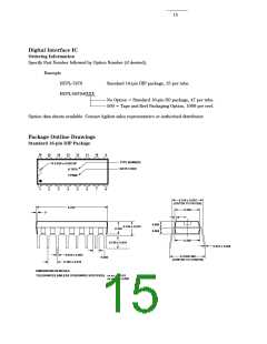
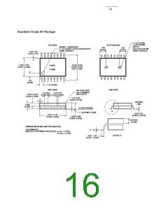
 ETC [ ETC ]