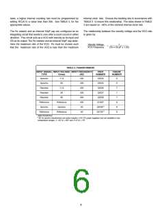
TABLE 1 notes:
1ꢀ Unused data bits are set to logic “0ꢀ”
clamps to the 5 VDC supplies. By performing the following
trigonometric identity, SINθ(COSφ) - COSθ(SINφ) = SIN(θ-φ),
the Control Transformer (CT) compares the analog input signals
( θ ) with the digital output ( φ ), resulting in an error signal pro-
portional to the sin of the angular difference. The CT uses a
combination of amplifiers, switches, logic and capacitors in pre-
cision ratios to perform the calculation.
.ꢀ In LVDT mode, Bit 3 is the MSB and resolution is
programmable to 8,10, 1., and 14 bitsꢀ
3ꢀ Accuracy in LVDT mode is 0ꢀ15% + 1 LSB of full scaleꢀ
4ꢀ In the frequency range of 47Hz to 1kHz, there will be
1 LSB of jitter at quadrant boundariesꢀ
5ꢀ The maximum phase shift tolerance will degrade linearly
from 45 degrees at 400 Hz to 30 degrees at 60 Hzꢀ
6ꢀ When using the -5V inverter, the VDD supply current will
double and VSSP can be up to .0% low, or -4Vꢀ
7ꢀ || = in parallel withꢀ
Note:The error output of the CT is normally sinusoidal, but
in LVDT mode, it is triangular (linear) and can be used to
convert any linear transducer output.
The converter accuracy is limited by the precision of the com-
puting elements in the CT. Instead of a traditional precision
resistor network, this converter uses capacitors with precisely
controlled ratios. Sampling techniques are used to eliminate
errors due to voltage drift and op-amp offsets.
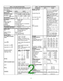
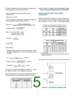
THEORY OF OPERATION
The RD-19230 is a mixed signal CMOS IC containing analog
input and digital output sections. Precision analog circuitry is
merged with digital logic to form a complete high-performance
tracking resolver-to-digital converter. For user flexibility and con-
venience, the converter bandwidth, dynamics, and velocity scal-
ing are externally set with passive components.
The error processing is performed using the industry standard
technique for Type II tracking converters. The DC error is inte-
grated yielding a velocity voltage which in turn drives a voltage
controlled oscillator (VCO). This VCO is an incremental integra-
tor (constant voltage input to position rate output) which, togeth-
er with the velocity integrator, forms a Type II servo feedback
loop. A lead in the frequency response is introduced to stabilize
the loop and another lag at higher frequency is introduced to
reduce the gain and ripple at the carrier frequency and above.
The settings of the various error processor gains and break fre-
quencies are done with external resistors and capacitors so that
the converter loop dynamics can be easily controlled by the user.
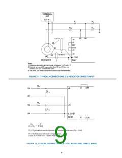
FIGURE 1 is the Functional Block Diagram of RD-19230. The
analog conversion electronics require 5 VDC power supplies,
and the converter contains a charge pump to provide the user
with the option of a single-ended +5 VDC supply. The converter
front-end consists of differential sine and cosine input amplifiers
which are protected up to 25 V with 2 kΩ resistors and diode
C
R
BW
B
VEL
C
/10
R
V
BW
VEL SJ1
VEL
-VCO
50 pf
C
VCO
CT
R
1
16 BIT
UP/DOWN
COUNTER
RESOLVER
INPUT
(θ)
+
VCO
GAIN
DEMOD
1
1ꢀ.5 V
THRESHOLD
-
C
F
S
S
11 mV/LSB
DIGITAL
OUTPUT
(φ)
H = 1
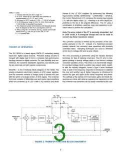
FIGURE 2. TRANSFER FUNCTION BLOCK DIAGRAM #1
3

 ETC [ ETC ]