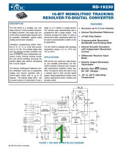
TABLE 1. RD-19230 SPECIFICATIONS (CONTINUED)
TABLE 1. RD-19230 SPECIFICATIONS
These specs apply over the rated power supply, temperature, and refer-
ence frequency ranges; 10ꢀ signal amplitude variation, and 10ꢀ har-
monic distortion.
PARAMETER
UNIT
VALUE
DIGITAL OUTPUTS
Parallel Data (1-16)
10, 12, 14, or 16 parallel lines;
natural binary angle positive
logic (see note 2)
0.25 to 0.75 µs positive pulse
leading edge initiates counter
update. (CB functions with
ZIP_EN pin tied to +5 V or NC)
Logic 1 at all 0’s
PARAMETER
RESOLUTION
UNIT
VALUE
Bits 10, 12, 14, or 16 (note 1 & 2)
Converter Busy (CB)
(4)
FREQUENCY RANGE
ACCURACY -XX2
-XX3 (note 3)
REPEATABILITY
Hz
47-1k
1k - 4k 4k - 10k
Min
Min
LSB
4 +1 LSB 4 +1 LSB 5 +1 LSB
2 +1 LSB 2 +1 LSB 3 +1 LSB
Zero Index Pulse (ZIP)
Built-In-Test (BIT)
1
1
1
1
2
2
(ZIP_EN pin tied to GND)
Logic 0 for BIT condition.
DIFFERENTIAL LINEARITY LSB
REFERENCE
Type
(+REF, -REF)
Differential
~
100 LSB’s of error with a fil-
ter of 500 µs, Loss of Signal
(LOS) less than 500 mV, or
Loss of Reference (LOR) less
than 500 mV
Incremental Encoder Output
50 pF+
Voltage: differential
single ended
overload
Vp-p 10 max.
Vp
5 max.
Vrms 25 continuous; 100 transient
Hz DC to 10k
Frequency
A, B
Ω
Input Impedance
10M min. || 20 pf
Drive Capability
SYNTHESIZED REFERENCE
(note 5)
Logic 0: 1 TTL load, 1.6 mA at
0.4 V max.
Sig/Ref Phase Shift Correction deg 45 max. from 400 Hz to 10kHz
Logic 1; 10 TTL loads, -0.4 mA
at 2.8 V min.
Logic 0; 100 mV max. driving
CMOS
Logic 1; +5 V supply minus
100 mV min. driving CMOS
High Z; 10 µA || 5 pF max.
SIGNAL INPUT
Type
(+S, -S, SIN, +C, -C, COS)
Resolver, differential,
groundbased
Voltage: operating
overload
Input impedance
Vrms
Vrms
Ω
2
15ꢀ
25 continuous
10M min || 10 pF.
DIGITAL INPUTS
TTL / CMOS Compatible
Inputs
DYNAMIC
CHARACTERISTICS
Resolution
(at maximum bandwidth)
Logic 0 = 0.8 V max.
Logic 1 = 2.0 V min.
Loading = 10 µA max P.U. cur-
rent source to +5 V || 5 pF max.
CMOS transient protected
bits
10
12
14
16
Tracking Rate (min)(note 6)
Bandwidth (Closed Loop)
Ka
A1
A2
A
B
rps
Hz
1152 288
72
18
1200 1200 600
300
2
1/sec
1/sec
1/sec
1/sec
1/sec
5.7M 5.7M 1.4M 360k
19.5 19.5 4.9 1.2
295k 295k 295k 295k
Inhibit (INH)
Logic 0 inhibits; Data stable with-
in 150 ns
2400 2400 1200
1200 1200 600
600
300
2k
Enable Bits 1 to 8 (EM)
Enable Bits 9 to 16 (EL)
Logic 0 enables; Data stable
within 150 ns
Logic 1 = High Impedance; Data
High Z within 100 ns
2
Acceleration (1 LSB lag)
Settling Time (179° step)
2M
2
500k 30k
20
deg/s
msec
8
50
VELOCITY
CHARACTERISTICS
Polarity
Resolution and Mode
Control (D1 & D0)
(See notes 1 & 2)
Mode D1 D0 Resolution
Positive for increasing angle
4 (at nominal power supply)
resolver
0
0
1
1
0
1
0
1
10 bits
12 bits
14 bits
16 bits
8 bits
Voltage Range (Full Scale)
Scale Factor Error
Scale Factor TC
Reversal Error
Linearity
Zero Offset
Zero Offset TC
Load
POWER SUPPLIES
Nominal Voltage
Voltage Range
Max Volt. w/o Damage
Current
V
ꢀ
10 typ
100 typ
0.75 typ
0.25 typ
5 typ
20 max
200 max
1.3 max
0.50 max
10 max
30 max
8 max
PPM/°C
ꢀ
ꢀ
mV
µV/°C
kΩ
LVDT -5V
0
0
1
-5V
-5V
10 bits
12 bits
14 bits
15 typ
-5V -5V
Logic 0 enables ZIP
Logic 1 enables CB
ZIP_EN
(note 6)
V
ꢀ
V
+5 (VDD)
-5 (VSS)
5
+7
5
-7
CMOS Compatable Inputs
Logic 0 = 1.5 V max.
Logic 1 = 3.5 V min.
negative voltage = -3.5 V min.
Logic 1 select VEL1 components
Logic 0 select VEL2 components
mA
25 max. (each)
TEMPERATURE RANGE
Operating
-30X
-20X
SHIFT
UP/DN
°C
°C
°C
0 to +70
-40 to +85
-40 to +85
Logic 1 will increase gain by 4
Logic 0 will decrease gain by 4
-5 V gain remains constant
Storage
PHYSICAL
CHARACTERISTICS
Size: 64-pin Quad Flat Pack in(mm)
WEIGHT
A QUAD B
Logic 0 enables encoder emulation
Falling edge latches encoder
resolution
0.52 x 0.52 (13.2 x 13.2)
0.018 ( 0.5 )
oz(g)
2

 ETC [ ETC ]