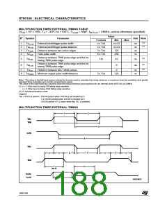
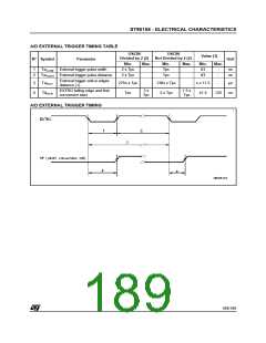
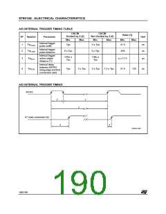
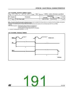
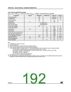
ST90158 - ELECTRICAL CHARACTERISTICS
A/D ANALOG SPECIFICATIONS
(V = 5V ± 10%, T = –40°C to +105°C, f
= 24MHz, unless otherwise specified)
DD
A
INTCLK
Parameter
Typical
Minimum
Maximum
Units (1)
INTCLK
INTCLK
µs
Notes
(2)(6)
Conversion time
Sample time
138
85
60
8
(6)
(6)
Power-up time
Resolution
8
bits
Monotonicity
GUARANTEED
No missing codes
Zero input reading
Full scale reading
Offset error
GUARANTEED
(6)
(6)
00
Hex
Hex
LSBs
LSBs
LSBs
LSBs
LSBs
kΩ
FF
0.5
0.6
0.6
1.0
(1)(4)(6)
(4)(6)
(4)(6)
(4)(6)
(4)(6)
(3)(5)(6)
(5)(6)
(6)
0.3
Gain error
DLE (Diff. Non Linearity error)
ILE (Int. Non Linearity error)
TUE (Absolute Accuracy)
Input Resistance
–1.0
1.0
2.7
1.3
1.4
0.8
Hold Capacitance
pF
Input Leakage
±1
µA
Note:
(1) “1LSBideal” has a value of AV /256
DD
(2) Including sample time
(3) This is the internal series resistance before the sampling capacitor
(4) This is a typical expected value, but not a tested production parameter.
If V(i) is the value of the i-th transition level (0 ≤ i ≤ 254), the performance of the A/D converter has been evaluated as follows:
OFFSET ERROR= deviation between the actual V(0) and the ideal V(0) (=1/2 LSB)
GAIN ERROR= deviation between the actual V(254) and the ideal V(254) - V(0) (ideal V(254)=AV -3/2 LSB)
DD
DNL ERROR= max {[V(i) - V(i-1)]/LSB - 1}
INL ERROR= max {[V(i) - V(0)]/LSB - i}
ABS. ACCURACY= overall max conversion error
(5) Simulated value, to be confirmed by characterisation.
(6) The specified values are guaranteed only if an overload condition occurs on a maximum of 2 non-selected analog input pins and the
absolute sum of input overload currents on all analog input pins does not exceed ±10 mA.
192/199
1

 ETC [ ETC ]