ST6200C/ST6201C/ST6203C
I/O PORT PIN CHARACTERISTICS (Cont’d)
11.8.2 Output Driving Current
Subject to general operating conditions for V , f
, and T unless otherwise specified.
DD OSC
A
Symbol
Parameter
Conditions
Min
Max
0.1
0.8
0.8
1.2
0.1
0.8
0.8
1.3
1.3
2
Unit
I
I
I
I
I
I
I
I
I
I
I
I
I
=+10µA, T ≤125°C
A
IO
IO
IO
IO
IO
IO
IO
IO
IO
IO
IO
IO
IO
=+3mA, T ≤125°C
Output low level voltage for a standard I/O pin
(see Figure 63 and Figure 66)
A
=+5mA, T ≤85°C
A
=+10mA, T ≤85°C
A
=+10µA, T ≤125°C
A
1)
V
OL
=+7mA, T ≤125°C
A
V
=+10mA, T ≤85°C
Output low level voltage for a high sink I/O pin
(see Figure 64 and Figure 67)
A
=+15mA, T ≤125°C
A
=+20mA, T ≤85°C
A
=+30mA, T ≤85°C
A
=-10µA, T ≤125°C
V
V
V
-0.1
A
DD
DD
DD
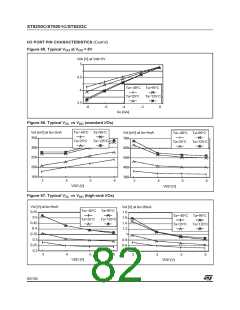
Output high level voltage for an I/O pin
(see Figure 65 and Figure 68)
2)
V
=-3mA, T ≤125°C
-1.5
-1.5
OH
A
=-5mA, T ≤85°C
A
Notes:
1. The I current sunk must always respect the absolute maximum rating specified in Section 11.2.2 and the sum of I
IO
IO
(I/O ports and control pins) must not exceed I
.
VSS
2. The I current source must always respect the absolute maximum rating specified in Section 11.2.2 and the sum of
IO
I
(I/O ports and control pins) must not exceed I
. True open drain I/O pins does not have V
.
IO
VDD
OH
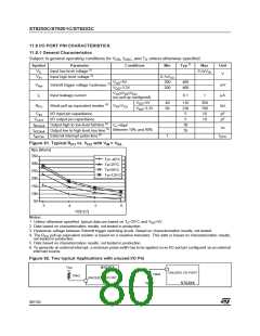
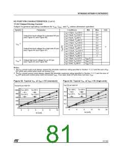
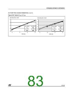
Figure 63. Typical V at V = 5V (standard)
Figure 64. Typical V at V = 5V (high-sink)
OL DD
OL
DD
Vol [V] at Vdd=5V
1
Vol [mV] at Vdd=5V
Ta=-40°C Ta=95°C
Ta=-40°C Ta=95°C
1000
800
600
400
200
0
0.8
0.6
0.4
0.2
0
Ta=25°C
Ta=125°C
Ta=25°C
Ta=125°C
0
4
8
12
16
20
0
2
4
6
8
10
Iio [mA]
Iio [mA]
81/104
1

 ETC [ ETC ]