ST6200C/ST6201C/ST6203C
11.8 I/O PORT PIN CHARACTERISTICS
11.8.1 General Characteristics
Subject to general operating conditions for V , f
, and T unless otherwise specified.
DD OSC
A
1)
Symbol
Parameter
Conditions
Min
Typ
Max
Unit
2)
V
Input low level voltage
0.3xVDD
IL
V
2)
V
Input high level voltage
0.7xVDD
200
IH
V
V
V
=5V
400
400
DD
3)
V
Schmitt trigger voltage hysteresis
Input leakage current
mV
µA
kΩ
hys
=3.3V
200
DD
SS≤V ≤V
IN
DD
I
0.1
1
L
(no pull-up configured)
V
V
=5V
40
80
110
230
5
350
700
10
DD
DD
4)
R
Weak pull-up equivalent resistor
V =V
IN SS
PU
=3.3V
C
I/O input pin capacitance
pF
pF
IN
C
I/O output pin capacitance
Output high to low level fall time
5
10
OUT
5)
5)
t
30
35
C =50pF
Between 10% and 90%
f(IO)out
L
ns
t
Output low to high level rise time
r(IO)out
6)
t
External interrupt pulse time
1
t
CPU
w(IT)in
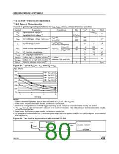
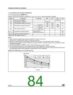
Figure 61. Typical R vs. V with V = V
SS
PU
DD
IN
Rpu [Khom]
350
Ta=-40°C
Ta=25°C
Ta=95°C
Ta=125°C
300
250
200
150
100
50
3
4
5
6
VDD [V]
Notes:
1. Unless otherwise specified, typical data are based on T =25°C and V =5V.
A
DD
2. Data based on characterization results, not tested in production.
3. Hysteresis voltage between Schmitt trigger switching levels. Based on characterization results, not tested.
4. The R pull-up equivalent resistor is based on a resistive transistor. This data is based on characterization results,
PU
not tested in production.
5. Data based on characterization results, not tested in production.
6. To generate an external interrupt, a minimum pulse width has to be applied on an I/O port pin configured as an external
interrupt source.
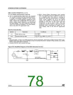
Figure 62. Two typical Applications with unused I/O Pin
V
ST62XX
DD
UNUSED I/O PORT
10kΩ
10kΩ
UNUSED I/O PORT
ST62XX
80/104
1

 ETC [ ETC ]