T1/E1 Short Haul Transceiver with Crystal-less Jitter Attenuation — LXT350
Contents
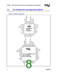
1.0
Pin Assignments and Signal Descriptions......................................................8
1.1 Mode Dependent Signals......................................................................................9
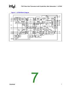
Functional Description...........................................................................................14
2.0
2.1
Initialization..........................................................................................................14
2.1.1 Reset Operation .....................................................................................14
Transmitter ..........................................................................................................14
2.2.1 Transmit Digital Data Interface...............................................................14
2.2.2 Transmit Monitoring................................................................................15
2.2.3 Transmit Drivers.....................................................................................15
2.2.4 Transmit Idle Mode.................................................................................15
2.2.5 Transmit Pulse Shape............................................................................15
Receiver ..............................................................................................................16
2.3.1 Receive Data Recovery..........................................................................16
2.3.2 Receive Digital Data Interface................................................................16
Jitter Attenuation .................................................................................................16
Hardware Mode...................................................................................................17
Host Mode...........................................................................................................17
2.6.1 Interrupt Handling...................................................................................17
Diagnostic Mode Operation.................................................................................19
2.7.1 Loopback Modes....................................................................................20
2.7.1.1 Local Loopback (LLOOP)..........................................................20
2.7.1.2 Analog Loopback (ALOOP).......................................................21
2.7.1.3 Remote Loopback (RLOOP) .....................................................22
2.7.1.4 Dual Loopback (DLOOP) ..........................................................23
2.7.2 Internal Pattern Generation....................................................................23
2.7.2.1 Transmit All Ones (TAOS).........................................................23
2.7.2.2 Quasi-Random Signal Source (QRSS) .....................................23
2.7.3 Error Insertion and Detection .................................................................25
2.7.3.1 Bipolar Violation Insertion (INSBPV).........................................25
2.7.3.2 Logic Error Insertion (INSLER)..................................................25
2.7.3.3 Logic Error Detection (QPD) .....................................................25
2.7.3.4 Bipolar Violation Detection (BPV)..............................................25
2.7.3.5 HDB3 Code Violation Detection (CODEV)................................25
2.7.3.6 HDB3 Zero Substitution Violation Detection (ZEROV)..............26
2.7.4 Alarm Condition Monitoring....................................................................26
2.7.4.1 Loss of Signal (LOS) .................................................................26
2.7.4.2 Alarm Indication Signal Detection (AIS) ....................................26
2.7.4.3 Driver Failure Monitor Open (DFMO)........................................27
2.7.4.4 Elastic Store Overflow/Underflow (ESOVR and ESUNF)..........27
2.7.4.5 Built-In Self Test (BIST).............................................................27
2.2
2.3
2.4
2.5
2.6
2.7
3.0
4.0
Register Definitions.................................................................................................28
Application Information.........................................................................................33
4.1
4.2
4.3
Transmit Return Loss..........................................................................................33
Transformer Data ................................................................................................33
Application Circuits..............................................................................................33
Datasheet
3

 ETC [ ETC ]