KT0803K
Operation Condition
Table 1: Operation Condition
Operating Condition
Relative to GND
Parameter
Symbol
Min
1.6
1.6
0
Typ
1.8
Max
2.0
3.6
70
Units
V
V
1.8V Analog Supply1 VDD
IO/Regulator Supply IOVDD
Relative to GND
Operating Temp
TA
Ambient Temperature
25
°C
Note: 1. No external voltage should be applied to this supply. Decoupling cap should be used instead
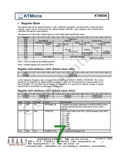
Specifications and Features
Table 2: FM Transmitter Functional Parameters (Unless otherwise noted TA = 0-70 oC,
IOVDD=1.6~3.6 V, Fin = 1 kHz)
Parameter
Symbol Test/Operating
Condition
Min
Nom
Max
Units
FM Frequency Range
Current Consumption
Ftx
IVDD
Pin 16
76
108
MHz
Pin 4 with PA (power
amp.) at default power
mode (PA_bias = 0,
RFGAIN[3:0]=1111)
Pin 4
Vin = 0.7 Vp-p, Gin = 0
Vin = 0.7 Vp-p, Gin = 0
Vin = 0.7 Vp-p, Gin = 0
Vin = 0.7 Vp-p, Gin = 0
Vin = 0.7 Vp-p, Gin = 0
Single-ended input
-
17
mA
Standby Current
Istand
-
-
-
0.1
60
0.3
-
40
-
1
-
μA
dB
%
dB
dB
dB
VRMS
dB
Signal to Noise Ratio
Total Harmonic Distortion
Left/Right Channel Balance
SNR
THD
BAL
-0.2
0.2
-
60
1.4
12
4
Stereo Separation (Left<->Right) SEP
Sub Carrier Rejection Ratio
SCR
Vin
Gin
Gstep
Vcm
-
-
-12
1
Input Swing1
0.35
0
PGA Range for Audio Input
PGA Gain Step for Audio Input
Required Input Common-Mode
Voltage when DC-coupled
Power Supply Rejection2
Ground Bounce Rejection2
Input Resistance (Audio Input)
Input Capacitance (Audio Input) Cin
Audio Input Frequency Band
Transmit Level
dB
Pin 5,7
0
0.8
1.8
V
PSRR
GSRR
Rin
IOVDD = 1.9 ~ 3.6 V
IOVDD = 1.9 ~ 3.6 V
Pin 5, 7
Pin 5, 7
Pin 5, 7
40
40
120
0.5
20
96
-
-
-
-
-
dB
dB
kΩ
pF
Hz
dBµV
kHz
kHz
kHz
150
0.8
-
103
50
7.5
180
1.2
15k
113
Fin
Vout
STEP
Channel Step
Pilot Deviation
Audio Deviation
Frequency Response
15
150
75
30
Mono,-3dB, ΔF=60kHz,
50/75μs pre-emphasis
SIG_PROC<1> = 1
SIG_PROC<0> = 0
Input clock
15k
Hz
Pre-emphasis Time Constant
Tpre
-
-
50
75
32.768
100
-
-
µs
µs
KHz
kHz
Crystal/External Clock
2-wire I2C Clock
High Level Input Voltage
CLK
SCL
VIH
Pin 14
Pin 4, 8, 12, 14, 16
0
400
0.75 x
IOVDD
IOVDD
+ 0.25
0.25 x
-
-
V
V
Low Level Input Voltage
VIL
Pin 4, 8, 12, 14, 16
- 0.25
IOVDD
DS-1896P-03 070604
深圳市圣邦达电子有限公司 传真:068-0755-61351350
联系人:邓 生 13798386757 QQ:278815928 E-MAIL:dengwangs@163.com
MSN:dengwangs@hotmail.com 网址:www.sbdsemi.com
2
本资料来源来自互联网,一切版权归属原设计公司,如有与法律相抵触之处,请及时联系我们,我们会及时修改更正

 ETC [ ETC ]