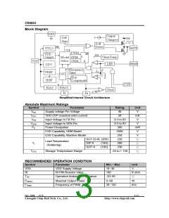
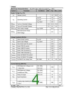
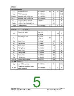
CR6853
the GATE pin operate again. So the
frequency of the internal OSC is invariable,
the register would reset some pulses so that
the practical frequency is decreased at the
GATE pin.
VIN
LP
value ( ∆I =
×TD ) due to the system
delay time that is from detecting the current
through the Sense pin to power MOSFET off
in the CR6853 (Among these, VIN is the
primary winding voltage of the transformer
and LP is the primary wind inductance). VIN
Internal Synchronized Slop
Compensation
ranges from 85VAC to 264VAC
.
To
Although there are more advantages of
the current mode control than conventional
voltage mode control, there are still several
drawbacks of peak-sensing current-mode
converter, especially the open loop
instability when it operates in higher than
50% of the duty-cycle. To solve this problem,
the CR6853 is introduced an internal slope
compensation adding voltage ramp to the
current sense input voltage for PWM
generation. It improves the close loop
stability greatly at CCM, prevents the
sub-harmonic oscillation and thus reduces
the output ripple voltage.
guarantee the output power is a constant for
universal input AC voltage, there is a
dynamic peak limit circuit to compensate the
system delay T that the system delay brings
on.
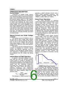
Vsense
1.10
1.05
1.00
0.95
0.90
0.85
0.80
0.75
0.70
Duty Cycle
0.65
DUTY
0% 10%20%30%40%50%60%70%80%90%
VSLOP = 0.33×
= 0.4389× DUTY
DUTYMAX
OLP&SCP
To protect the circuit from being
damaged under the over load or short circuit
condition, a smart OLP&SCP function is
implemented in the CR6853. When short
circuit or over load occurs in the output end,
the feedback cycle would enhance the
voltage of FB pin, while the voltage is over
3.7V or the current from FB is below 170uA,
the internal detective circuit would send a
signal to shut down the GATE and pull down
the VDD voltage, then the circuit is restart.
To avoid the wrong operation when circuit
starts, the delay time is set. When the RI
resistance is 100Kohm, the delay time
TOLP&SCP is between 33mS and 50mS. The
relationship between RI and TOLP&SCP
follows the below equation.
Slop Compensation
Current Sensing & Dynamic peak
limiting
The current flowing by the power
MOSFET comes into being a voltage VSENSE
on the Sense pin cycle-by-cycle, which
compares to the internal reference voltage,
and controls the reverse of the internal
register, limits the peak current IMAX of the
primary of the transformer. The transformer
RI ×
2
RI ×3
6×
103
(
mS
)
< TOLP
<
SCP
(mS)
&
6
×
103
1
energy is E = × L × IMAX 2 . So adjusting
2
the RSENSE can set the maximal output
power of the power supple. The current
flowing by the power MOSFET has an extra
Oct, 2008 V2.0
7/12
Chengdu Chip-Rail Tech. Co., Ltd.
http://www.chiprail.com

 ETC [ ETC ]