PRELIMINARY PRODUCT SPECIFICATION
nRF24L01 Single Chip 2.4 GHz Radio Transceiver
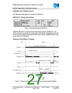
IMPORTANT TIMING DATA
The following timing applies for operation of nRF24L01.
nRF24L01 Timing Information
nRF24L01 timing
Power Down ꢀ Standby mode
Standby modes ꢀ TX/RX mode
Minimum CE high
Max.
1.5ms
130µs
Min.
Name
Tpd2stby
Tstby2a
Thce
Tpece2csn
10µs
4µs
Delay from CE pos. edge to CSN low
Table 13 Operational timing of nRF24L01
When the nRF24L01 is in power down it must always settle in Standby for 1.5ms
before it can enter one of the TX or RX modes. Note that the configuration word will
be lost if VDD is turned off and that the device then must be configured before going
to one of the TX or RX mode.
Enhanced ShockBurst™ timing
0us
250us
1
2
1 byte payload with ACK (339 us)
ESB cycle
CE high minimum 10 us
PTX: CE
PTX: IRQ (TX_DS)
2 us
STBY I
TX
RX
TX
PTX: Mode
Antenna
6 us
ACK (33 us)
Payload (33 us + 4 us/byte)
128 us
1
0
PRX: CE
PRX: IRQ (RX_DR)
PRX: Mode
6 us
SPI: IRQ Clear
128 us
STBY I
RX
TX
RX
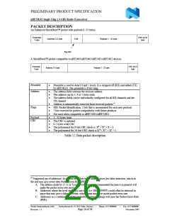
Packet:
Address: 5 bytes
CRC: 1 byte
Payload: 1 byte
Figure 11 Timing of Enhanced ShockBurst™ for one packet upload (2Mbps).
Nordic Semiconductor ASA - Vestre Rosten 81, N-7075 Tiller, Norway
Revision: 1.1
-
Phone +4772898900
-
Fax +4772898989
November 2005
Page 27 of 38

 ETC [ ETC ]