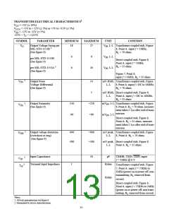
1
TRANSMITTER ELECTRICAL CHARACTERISTICS
V
V
V
= +5V (± 10%)
CC
= +5V to + 12V (± 5%) or +5V to +15V (± 5%)
CCA
= -12V or -15V (± 5%)
EE
-55°C < T < +125°C
C
SYMBOL
PARAMETER
MINIMUM
MAXIMUM
UNIT
CONITION
V
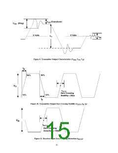
Output Voltage Swing per
MIL-STD-1553B
(See figure 9)
18
27
V
V
V
L-L Transformer-coupled stub, Figure
O
PP,
PP,
PP,
2
8, Point A: input ¦ = 1MHz,
R = 70 ohms.
L
6
6
9
L-L
L-L
per MIL-STD-1553B
(See figure 9)
Direct-coupled stub, Figure 8,
Point A: input ¦ = 1MHz,
R = 35 ohms.
2
L
per MIL-STD-1553A
20
(See figure 9)
Figure 7, Point A:
input ¦ = 1MHz, R = 35 ohms.
L
2
V
Output Noise
Voltage Differential
(See figure 9)
14
5
mV-RMS, Transformer-coupled stub, Figure
L-L 8, Point A: input ¦ = DC to 10MHz,
R = 70 ohms.
NS
L
mV-RMS, Direct-coupled stub, Figure 8,
L-L Point A: input ¦ = DC to 10MHz,
R = 35 ohms.
L
Output Symmetry
(See figure 9)
-250
-90
+250
+90
mV , L-L Transformer-coupled stub, Figure
PP
2
V
OS
8, Point A: R = 70 ohms, measure-
L
ment taken 2.5ms after end of trans-
mission
mV , L-L
PP
Direct-coupled stub, Figure 8,
Point A: R = 35 ohms, measure-
L
ment taken 2.5ms after end of trans-
mission
2
Output voltage distortion
(overshoot or ring)
(See figure 9)
-900
-300
+900
+300
mV peak, Transformer-coupled stub, Figure
L-L 8, Point A: R = 70 ohms.
V
DIS
L
mV peak, Direct-coupled stub, Figure 8,
L-L
Point A: R = 35 ohms.
L
Input Capacitance
10
pF
TXIHB, TXIN, TXIN; input
¦ = 1MHz @ 0 V
2
C
IN
Terminal Input Impedance
1
2
Kohm
2
Transformer-coupled stub, Figure
7, Point A: input ¦ = 75KHz to
1MHz (power on or power off: non-
T
IZ
transmitting, R removed from
L
Kohm
circuit).
Direct-coupled stub, Figure 6,
Point A: input ¦ = 75KHz to 1MHz
(power on or power off: non-trans-
mitting, R removed from circuit).
L
Notes:
1. All tests guaranteed per test figure 6.
2. Guaranteed by device characterization.
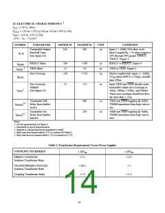
13

 ETC [ ETC ]