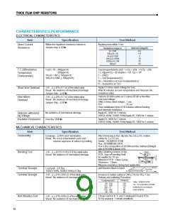
THICK FILM CHIP RESISTORS
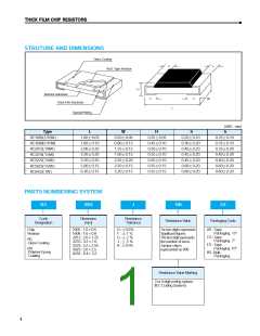
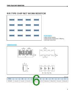
STRUTURE AND DIMENSIONS
Glass Coating
1
1
l
l
2
RuO Type Resistor
H
Alumina Substrate
2
2
l
l
W
Thick-Film Electrode
L
Special Plating
(
:
)
UNIT mm
Type
L
W
H
I1
I2
RC1005(1/16W )
RC1608(1/10W)
RC2012( 1/8W )
RC3216( 1/4W)
RC3225( 1/4W )
RC5025( 1/2W )
RC6432( 1W )
1.00±0.05
1.60±0.10
2.00±0.20
3.20±0.20
3.20±0.20
5.00±0.15
6.30±0.15
0.50±0.05
0.80±0.15
1.25±0.15
1.60±0.15
2.55±0.20
2.50±0.15
3.20±0.15
0.35±0.05
0.45±0.10
0.50±0.10
0.55±0.10
0.55±0.10
0.55±0.15
0.55±0.15
0.20±0.10
0.30±0.20
0.40±0.20
0.45±0.20
0.45±0.20
0.60±0.20
0.60±0.20
0.25±0.10
0.35±0.10
0.35±0.20
0.40±0.20
0.40±0.20
0.60±0.20
0.60±0.20
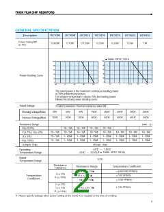
PARTS NUMBERING SYSTEM
R C
2012
J
100
CS
1
2
3
4
5
Dimension
(mm)
Resistance
Tolerance
Code
Designation
Resistance Value
Packaging Code
:
AS Tape
:
:
:
:
:
Chip
1005 1.0×0.5
D ±0.5%
1st two digits represents
Significant figures.
The last digit represents
the number of zeros.
Jumper chip is
Packaging. 13”
:
Resistor
1608 1.6×0.8
F ±1 %
:
CS Tape
:
2012 2.0×1.25
G ±2 %
-RC
:
Packaging. 7”
ES Tape
Packaging. 10”
:
3216 3.2×1.6
J ±5 %
Glass Coating
:
:
:
K ±10%
3225 3.2×2.55
-RH
:
:
5025 5.0×2.5
represented as 000
Polymer Epoxy
Coating
:
BS Bulk
:
6432 6.4×3.2
Packaging.
Resistance Value Marking
3 or 4 digit coding system.
(
IEC Coding System)
4

 ETC [ ETC ]