Data Sheet
June 1999
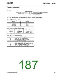
ORCA Series 2 FPGAs
Reconfiguration (see FPGA States of Operation)
Routing
Index (continued)
3-Statable Bidirectional Buffers, 17—18, 148
Clock Routing, 24, 149—153
(see also Clock Distribution Network)
Configurable Interconnect Points (CIPs), 17
Fast-Carry Routing, 24
Inter-PLC Routing Resources, 18—19
Interquad Routing, 5, 17, 32—36
Intra-PLC Routing Resources, 18
Minimizing Routing Delay, 20
160-Pin QFP, 177
208-Pin SQFP, 178
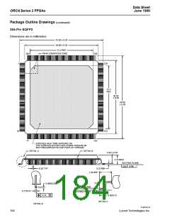
208-Pin SQFP2, 179
240-Pin SQFP, 180
240-Pin SQFP2, 181
256-Pin PBGA, 182
304-Pin SQFP, 183
304-Pin SQFP2, 184
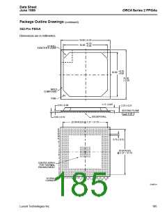
352-Pin PBGA, 185
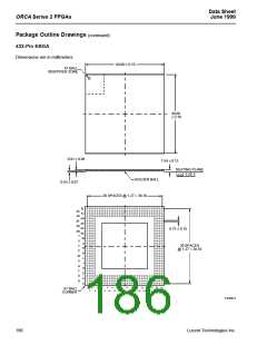
432-Pin EBGA, 186
Terms and Definitions, 173
PLC Routing, 17—24, 34
Programmable Corner Cell Routing, 37
PIC Routing, 27—31
Pin Information, 71—125
84-Pin PLCC, 71
100-Pin TQFP, 73
144-Pin TQFP, 75
S
Boundary Scan, 54–59
Global 3-State Control (TS_ALL), 37, 66
Global Set/Reset (GSRN), 7, 16, 37
Internal Oscillator, 37
160-Pin QFP, 77
208-Pin SQFP/SQFP2, 81
240-Pin SQFP/SQFP2, 86
256-Pin PBGA, 92
Readback Logic, 37
Start-up, 41 (see also FPGA States of Operation)
Subtractor (see LUT Operating Modes)
System Clock (see Clock Distribution Network)
304-Pin SQFP/SQFP2, 99
352-Pin PBGA, 106
432-Pin EBGA Pinout, 116
Package Compatibility, 68—70
Pin Descriptions, 71
T
Power Dissipation, 61—65
5 V Tolerant I/O, 64
3-state (see Bidirectional Buffers, TS_ALL)
Timing Characteristics, 132–168
Asynchronous Peripheral Configuration Mode, 163
Boundary-Scan Timing, 168
OR2CxxA, 61
OR2TxxA, 63
Programmable Function Unit (PFU), 5—16
Control Inputs, 5, 7
Operating Modes, 7—15
Latches/Flip-Flops, 15—16
Programmable Input/Output Cells (PICs), 25—31
5 V Tolerant I/O, 26
Clock Timing, 149
General Configuration Mode Timing, 158
Master Parallel Configuration Mode, 162
Master Serial Configuration Mode, 161
PFU Timing, 132
PIO Timing, 154
Architecture, 29—30
Inputs, 25
PLC Timing, 148
Readback Timing, 167
Outputs, 26
Slave Parallel Configuration Mode, 166
Slave Serial Configuration Mode, 165
Tolerant I/O, 26 (see also 5 V Tolerant I/O)
TS_ALL, 1, 37, 66
Open-Drain Output Option, 26
Propagation Delays, 26
Overview, 25
Zero-Hold Input, 25
U—Z
Programmable Logic Cells (PLCs), 5—24
Architecture, 22—24
Latches/Flip-Flops, 15—16
PFU, 5—16
Zero-hold Inputs, 25
Routing, 17—24
R
RAM (see also FPGA Configuration), 17, 44, 135, 142
Dual-port, 3, 7, 13—15
Single-port, 3, 7, 12—15
Recommended Operating Conditions, 129
Lucent Technologies Inc.
190

 ETC [ ETC ]