Data Sheet
June 1999
ORCA Series 2 FPGAs
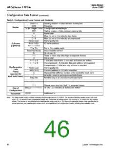
FPGAs. Following the header frame is an optional ID
frame. This frame contains data used to determine if
the bit stream is being loaded to the correct type of
ORCA FPGA (i.e., a bit stream generated for an
OR2C15A is being sent to an OR2C15A). Since the
OR2CxxA devices are bit stream compatible with the
ATT2Cxx, ATT2Txx, OR2TxxA, and OR2TxxB families,
a bit stream from any of these devices will not cause an
error when loaded into an OR2CxxA, OR2TxxA, or
OR2TxxB device. The ID frame has a secondary func-
tion of optionally enabling the parity checking logic for
the rest of the data frames.
Configuration Data Format (continued)
Using ORCA Foundry to Generate
Configuration RAM Data
The configuration data defines the I/O functionality,
logic, and interconnections. The bit stream is gener-
ated by the development system. The bit stream cre-
ated by the bit stream generation tool is a series of 1s
and 0s used to write the FPGA configuration RAM. The
bit stream can be loaded into the FPGA using one of
the configuration modes discussed later. In the bit
stream generator, the designer selects options which
affect the FPGA’s functionality. Using the output of the
bit stream generator, circuit.bit, the development sys-
tem’s download tool can load the configuration data
into the ORCA series FPGA evaluation board from a
PC or workstation. Alternatively, a user can program a
PROM (such as the ATT1700A Series Serial ROM or a
standard EPROM) and load the FPGA from the PROM.
The development system’s PROM programming tool
produces a file in .mks or .exo format.
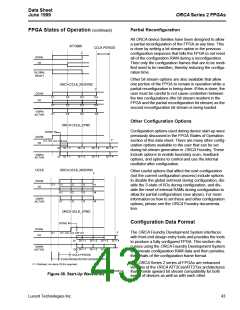
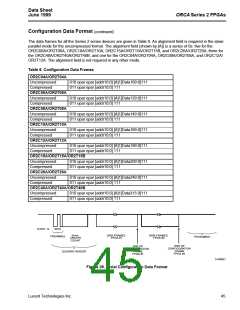
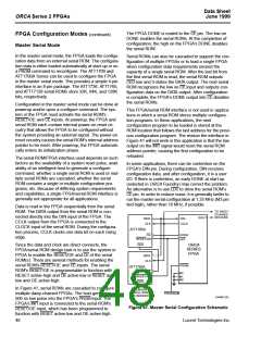
The configuration data frames follow. Each frame starts
with a 0 start bit and ends with three or more 1 stop
bits. Following each start bit are four control bits: a pro-
gram bit, set to 1 if this is a data frame; a compress bit,
set to 1 if this is a compressed frame; and the opar and
epar parity bits (see Bit Stream Error Checking). An
11-bit address field that determines in which column
the FPGA is to be written is followed by alignment and
write control bits. For uncompressed frames, the data
bits needed to write one column in the FPGA are next.
For compressed frames, the data bits from the previous
frame are sent to a different FPGA column, as speci-
fied by the new address bits; therefore, new data bits
are not required. When configuration of the current
FPGA is finished, an end-of-configuration frame (where
the program bit is set to 0) is sent to the FPGA. The
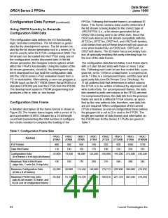
length and number of data frames and information on
the PROM size for the Series 3 FPGAs are given in
Table 7.
Configuration Data Frame
A detailed description of the frame format is shown in
Figure 39. The header frame begins with a series of 1s
and a preamble of 0010, followed by a 24-bit length
count field representing the total number of configura-
tion clocks needed to complete the loading of the
Table 7. Configuration Frame Size
OR2C/
2T04A
OR2C/
2T06A
OR2C/
2T08A
OR2C/
2T10A
OR2C/
2T12A
OR2C/
2T15A/B
OR2C/
2T26A
OR2C/
2T40A/B
Devices
# of Frames
480
110
568
130
656
150
744
170
832
190
920
210
1096
250
1378
316
Data Bits/Frame
Configuration Data
52,800
73,840
98,400
126,480 158,080 193,200 274,000 435,448
(# of frames x # of data bits/frame)
Maximum Total # Bits/Frame
136
160
176
200 216 240 280 344
(align bits, 1 write bit, 8 stop bits)
Maximum Configuration Data
(# bits x # of frames)
65,280
65,504
90,880
91,128
115,456 148,800 179,712 220,800 306,880 474,032
115,720 149,088 180,016 221,128 307,248 474,464
Maximum PROM Size (bits)
(add 48-bit header, ID frame, and
40-bit end of configuration frame)
44
Lucent Technologies Inc.

 ETC [ ETC ]