Data Sheet
June 1999
ORCA Series 2 FPGAs
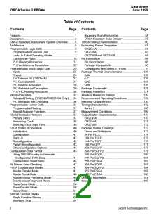
Contents
Table of Contents
Page Contents
Page
Features ......................................................................1
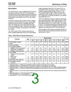
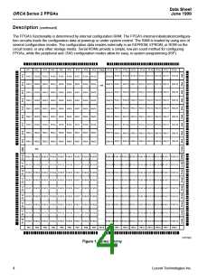
Description...................................................................3
ORCA Foundry Development System Overview.........5
Architecture .................................................................5
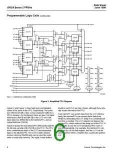
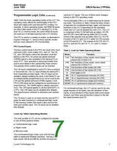
Programmable Logic Cells ..........................................5
Programmable Function Unit...................................5
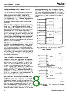
Look-Up Table Operating Modes ............................7
Latches/Flip-Flops .................................................15
PLC Routing Resources ........................................17
PLC Architectural Description................................22
Programmable Input/Output Cells .............................25
Inputs.....................................................................25
Outputs..................................................................26
5 V Tolerant I/O (OR2TxxB) ..................................27
PCI Compliant I/O..................................................27
PIC Routing Resources.........................................28
PIC Architectural Description.................................29
PLC-PIC Routing Resources.................................30
Interquad Routing......................................................32
Subquad Routing (OR2C40A/OR2T40A Only)......34
PIC Interquad (MID) Routing .................................36
Programmable Corner Cells......................................37
Programmable Routing..........................................37
Special-Purpose Functions....................................37
Clock Distribution Network ........................................37
Primary Clock ........................................................37
Secondary Clock ...................................................38
Selecting Clock Input Pins.....................................39
FPGA States of Operation.........................................40
Initialization............................................................40
Configuration .........................................................41
Start-Up .................................................................42
Reconfiguration .....................................................42
Partial Reconfiguration ..........................................43
Other Configuration Options..................................43
Configuration Data Format ........................................43
Using ORCA Foundry to Generate
Boundary-Scan Instructions...................................55
ORCA Boundary-Scan Circuitry ............................56
ORCA Timing Characteristics....................................60
Estimating Power Dissipation ....................................61
OR2CxxA...............................................................61
OR2TxxA ...............................................................63
OR2T15B and OR2T40B.......................................65
Pin Information ..........................................................66
Pin Descriptions.....................................................66
Package Compatibility ...........................................68
Compatibility with Series 3 FPGAs........................70
Package Thermal Characteristics............................126
QJA......................................................................126
yJC.......................................................................126
QJC......................................................................126
QJB......................................................................126
Package Coplanarity ...............................................127
Package Parasitics..................................................127
Absolute Maximum Ratings.....................................129
Recommended Operating Conditions......................129
Electrical Characteristics .........................................130
Timing Characteristics .............................................132
Series 2................................................................160
Measurement Conditions.........................................169
Output Buffer Characteristics...................................170
OR2CxxA.............................................................170
OR2TxxA .............................................................171
OR2TxxB .............................................................172
Package Outline Drawings ......................................173
Terms and Definitions..........................................173
84-Pin PLCC........................................................174
100-Pin TQFP......................................................175
144-Pin TQFP......................................................176
160-Pin QFP........................................................177
208-Pin SQFP......................................................178
208-Pin SQFP2....................................................179
240-Pin SQFP......................................................180
240-Pin SQFP2....................................................181
256-Pin PBGA .....................................................182
304-Pin SQFP......................................................183
304-Pin SQFP2....................................................184
352-Pin PBGA .....................................................185
432-Pin EBGA .....................................................186
Ordering Information................................................187
Index........................................................................189
Configuration RAM Data.....................................44
Configuration Data Frame .....................................44
Bit Stream Error Checking.........................................47
FPGA Configuration Modes.......................................47
Master Parallel Mode.............................................47
Master Serial Mode ...............................................48
Asynchronous Peripheral Mode ............................49
Synchronous Peripheral Mode ..............................49
Slave Serial Mode .................................................50
Slave Parallel Mode...............................................50
Daisy Chain ...........................................................51
Special Function Blocks ............................................52
Single Function Blocks ..........................................52
Boundary Scan......................................................54
2
Lucent Technologies Inc.

 ETC [ ETC ]