CY545 Stepper System Controller
www.ControlChips.com
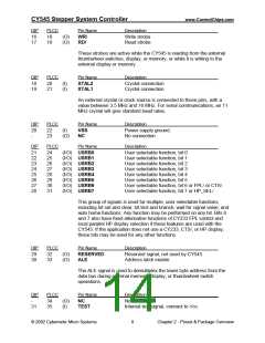
DIP
PLCC
Pin Name
Description
32
33
34
35
36
37
38
39
36
37
38
39
40
41
42
43
(I/O) D7
Parallel data bus, bit 7, MSB
Parallel data bus, bit 6
Parallel data bus, bit 5
Parallel data bus, bit 4
Parallel data bus, bit 3
Parallel data bus, bit 2
Parallel data bus, bit 1
Parallel data bus, bit 0, LSB
(I/O) D6
(I/O) D5
(I/O) D4
(I/O) D3
(I/O) D2
(I/O) D1
(I/O) D0
This group is the parallel data bus, used to read or write parallel data.
During access to external thumbwheel switches, memory, or display, the
lower byte of the device address is presented on these lines just prior to
the data transfer. Parallel commands are also accepted by the CY545 on
these lines, using the handshake control signals. These lines are open
drain, so external pull-up resistors are required when they are used as
outputs.
DIP
40
PLCC
44
Pin Name
VCC
Description
+5 Volt power supply input.
(I)
© 2002 Cybernetic Micro Systems
10
Chapter 2 - Pinout & Package Overview

 ETC [ ETC ]