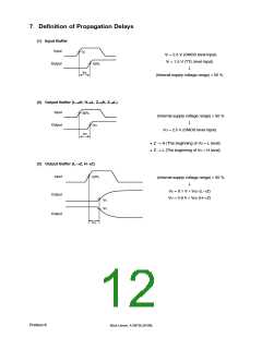
3. Propagation DelayTime (tPD)
The method shown here is a simplified calculation formula. This calculation method will give comparatively
accurate results when the load matches the following conditions. The error becomes greater as the load
capacitance increases, and the results yielded from the calculation are smaller than the values obtained from the
simulator. Therefore, note beforehand that these values should be used mainly as a general guide.
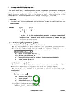
Conditions
The total F/I of the front stage of the block for delay calculation shall be within 15% of the F/O limit of the front
stage drive block.
Block A
Block B
Example
Let block B be the object of the propagation calculation. The accuracy of the simplified
calculation formula is high when the sum of the F/I connected to the output of Block A is
within 15% of the block A F/O limit.
3.1 Calculating Propagation Delay Time
3.1.1 Delay time of input buffer and internal function block
The delay time of input buffer and internal function block can be estimated from the load (number of fan-
outs) connected to the block including the memory block and its wiring length (wiring capacitance).
tPD = tLD0 + (ΣF/O + L) × t1
(ns)
tLD0
: Delay time of block itself when F/O = 0, L = 0
ΣF/O : Number of fan-outs of output pin
L
: Wiring capacitance of output pin (see the 3.1.3 Estimated Wiring Capacitance)
t1
: Delay coefficient of output pin
3.1.2 Delay time of output buffer
The delay time of an output buffer greatly depends on the load capacitance connected to the output pin.
The dependency of delay time on load capacitance varies with the drive capability of the buffer.
The delay time(tPD) of an output buffer can be estimated for the given load capacitance(CL) using the
following formula:
tPD = tLD0 + T × CL (ns)
tLD0
T
: Reference delay time (ns)
: Delay coefficient
CL
: Load capacitance (pF) (CL ≥ 15 pF)
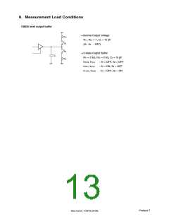
The delay time of an I/O buffer is obtained as follows.
CMOS level interface : Threshold voltage = 1/2 VDD
Preface-3
Block Library A13872EJ5V0BL

 ETC [ ETC ]