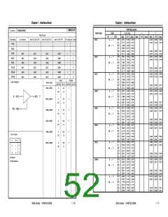
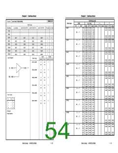
Chapter 1 Interface Block
Chapter 1 Interface Block
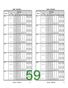
Switching speed
t LD0 (ns)
CMOS 5.0 V
Function
N-ch open drain Buffer
Block type
Path
→
t 1
T
Block type
IN
OUT
MIN.
0.361
0.264
0.361
0.264
0.361
0.264
0.424
0.259
0.424
0.259
0.424
0.259
0.547
0.266
0.547
0.266
0.547
0.266
0.672
0.275
0.672
0.275
0.672
0.275
TYP. MAX. MIN.
TYP. MAX. MIN.
TYP. MAX.
Drivability
1mA
no resistor
with 50 KΩ P/D
with 50 KΩ P/U
with 5 KΩ P/U
I/O cells int. Cells
(LZ)
(ZL)
(LZ)
(ZL)
(LZ)
(ZL)
(LZ)
(ZL)
(LZ)
(ZL)
(LZ)
(ZL)
(LZ)
(ZL)
(LZ)
(ZL)
(LZ)
(ZL)
(LZ)
(ZL)
(LZ)
(ZL)
(LZ)
(ZL)
0.465
0.493
0.465
0.493
0.465
0.493
0.546
0.479
0.546
0.479
0.546
0.479
0.707
0.485
0.707
0.485
0.707
0.485
0.864
0.498
0.864
0.498
0.864
0.498
0.633
1.001
0.633
1.001
0.633
1.001
0.714
0.914
0.714
0.914
0.714
0.914
0.885
0.860
0.885
0.860
0.885
0.860
1.051
0.848
1.051
0.848
1.051
0.848
EXT1
EXT3
EXW3
EXT9
EXTB
EXWB
EXT5
EXT7
EXW7
EXTD
EXTF
EXWF
A
A
A
A
A
A
A
A
A
A
A
A
→
→
→
→
→
→
→
→
→
→
→
→
Y
Y
Y
Y
Y
Y
Y
Y
Y
Y
Y
Y
0.026
0.026
0.026
0.020
0.020
0.020
0.014
0.014
0.014
0.011
0.011
0.011
0.035
0.035
0.035
0.026
0.026
0.026
0.019
0.019
0.019
0.015
0.015
0.015
0.050
0.050
0.050
0.038
0.038
0.038
0.026
0.026
0.026
0.021
0.021
0.021
2mA
3mA
6mA
9mA
EXT1
EXT9
EXT5
EXTD
EXT3
EXTB
EXT7
EXTF
EXW3
EXWB
EXW7
1
1
1
1
4
4
4
4
12mA
18mA
24mA
EXWF
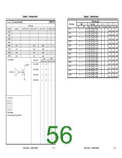
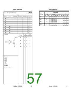
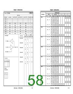
Input
Output
Logic Diagram
Block type
EXT1 to EXW3
Symbol Fan-in Symbol Fan-out
A
A
A
A
6.2
6.2
6.2
6.2
Y
Y
Y
Y
-
-
-
-
N01
Y
EXT9 to EXWB
EXT5 to EXW7
EXTD to EXWF
A
H01
Truth Table
A
Y
1
0
Z
0
Z:High Impedance
Connect a pull-up resistor to get a high level
Block Library A13872EJ5V0BL
1 - 24
Block Library A13872EJ5V0BL
1 - 25

 ETC [ ETC ]