Preliminary
RT9261B
Absolute Maximum Ratings
z Output Voltage
z LX Pin Voltage
8V
8V
-0.3 to V
(1)
z CE Pin Voltage
+0.3V
OUT
z LX Pin Output Current
400mA
z Power Dissipation, P @ T = 25°C
D
A
SOT-89
SOT-25
0.5W
0.25W
z Package Thermal Resistance
SOT-89, θ
SOT-89, θ
SOT-25, θ
100°C/W
300°C/W
250°C/W
JC
JA
JA
z Operating Temperature Range
z Storage Temperature Range
z Lead Temperature (Soldering, 10 sec.)
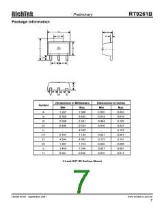
Notes: (1) Applicable to RT9261B-xxCB
-20 to +85°C
-65°C to 150°C
260°C
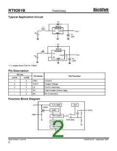
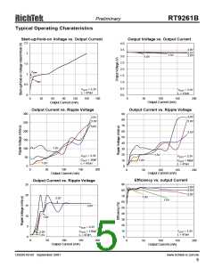
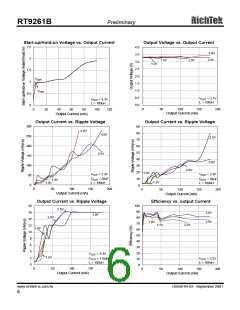
Electrical Characteristics (Refer to Fig. 1)
Parameter
Output Voltage Accuracy
Input Voltage
Symbol
∆V
Test Conditions
Min Typ Max Units
-2
--
--
--
+2
7
%
V
V
V
OUT
V
V
V
IN
Start-up Voltage
--
0.8
--
1
I
I
= 1mA, V : 0 → 2V
IN
ST
OUT
Hold-on Voltage
0.7
--
--
= 1mA, V : 2 → 0V
HO
OUT
IN
(1)
24
36
36
45
V
≤ 3.5V
OUT
To be measured at V in
IN
Input Current 1
Input Current 2
µA
µA
(2)
continuous switching
--
3.5V < V
≤ 5V
OUT
To be measured at V
switch off condition
in
(1) (2)
OUT
--
6.5
10
(1)
To be measured at V in
IN
--
--
18
20
36
45
V
≤ 3.5V
OUT
Input Current 3
µA
no load (guaranteed by I
1
(2)
(2)
3.5V < V
≤ 5V
(1)
OUT
and I )
2
120
160
--
--
--
--
--
V
OUT
≤ 3.5V
LX Switching Current
LX Leakage Current
mA
I
I
V
LX
= 0.4V
SWITCHING
3.5V < V
≤ 5V
OUT
--
0.5
µA
V
LX
= 6V
LEAKAGE
Maximum Oscillator Frequency
Oscillator Duty Cycle
Efficiency
140
65
190
75
80
0.8
240 KHz
F
MAX
85
--
%
%
V
D
On (V “L”) side
OSC
LX
--
LX switch on
0.65
1.0
V
LX
Voltage Limit
Notes:
(1) V = 1.8V, V = 0V, I = 1mA, Topt = 25°C, and External Circuit of Typical Application
OUT
IN
SS
(2) V = 3V, V = 0V, I = 1mA, Topt = 25°C, and External Circuit of Typical Application
IN
SS
OUT
DS9261B-03 September 2001
www.richtek-ic.com.tw
3

 ETC [ ETC ]