RT9261B
Preliminary
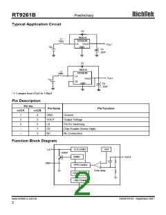
Typical Application Circuit
D1
1N5819
RT9261B
L1
LX
VOUT
GND
V
OUT
µ
V
IN
27 H
+
Co
µ
22 F
-
D1
1N5819
L1
RT9261B
LX
µ
27 H
V
OUT
VOUT
GND
V
IN
CE
+
Co
µ
22 F
-
* L1 ranges from 27µH to 120µH
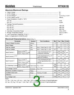
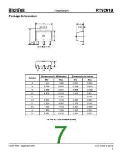
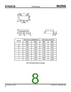
Pin Description
Pin No.
Pin Name
Pin Function
-xxCX
-xxCB
1
2
4
2
5
1
3
GND
VOUT
LX
Ground
Output Voltage
3
Pin for Switching
--
--
CE
Chip Enable (Active High)
No Connection
NC
Function Block Diagram
VLX Limiter
Vref
LX
LXSW
Buffer
VOUT
GND
-
+
VFM Control
Error Amp.
OSC 190kHz
Chip Enable
CE
www.richtek-ic.com.tw
DS9261B-03 September 2001
2

 ETC [ ETC ]