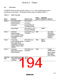
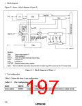
2. Block diagram
Figure 9-1 shows a block diagram of timer A.
CWORS
øW
1/4
PSW
TMA
øW/4
øW/32
øW/16
øW/8
øW/128
øW/4
TCA
TMOW
ø/32
ø/16
ø/8
ø/8192, ø/4096, ø/2048,
ø/512, ø/256, ø/128,
ø/32, ø/8
ø/4
ø
PSS
IRRTA
Notation:
TMA:
TCA:
Timer mode register A
Timer counter A
IRRTA:
PSW:
PSS:
Timer A overflow interrupt request flag
Prescaler W
Prescaler S
CWOSR: Subclock output select register
Note: * Can be selected only when the prescaler W output (øW/128) is used as the TCA input clock.
Figure 9-1 Block Diagram of Timer A
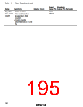
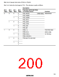
3. Pin configuration
Table 9-2 shows the timer A pin configuration.
Table 9-2 Pin Configuration
Name
Abbrev.
I/O
Function
Clock output
TMOW
Output
Output of waveform generated by timer A output circuit
182

 ETC [ ETC ]