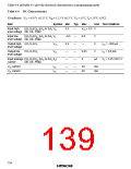
Table 6-5 AC Characteristics
(Conditions: VCC = 6.0 V ±0.25 V, VPP = 12.5 V ±0.3 V, Ta = 25°C ±5°C)
Item
Symbol Min Typ Max Unit Test Condition
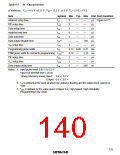
Address setup time
OE setup time
tAS
2
—
—
—
—
—
—
—
—
—
—
—
—
130
—
µs Figure 6-5*1
tOES
tDS
2
µs
µs
µs
µs
µs
µs
Data setup time
Address hold time
Data hold time
2
tAH
0
tDH
2
Data output disable time
VPP setup time
tDF*2
tVPS
tPW
—
2
Programming pulse width
0.19 0.20 0.21 ms
3
PGM pulse width for overwrite programming tOPW
*
0.19
—
—
—
—
5.25 ms
CE setup time
tCES
tVCS
tOE
2
2
0
—
µs
µs
ns
VCC setup time
—
Data output delay time
200
Notes: 1. Input pulse level: 0.45 V to 2.2 V
Input rise time/fall time ≤ 20 ns
Timing reference levels Input: 0.8 V, 2.0 V
Output: 0.8 V, 2.0 V
2. tDF is defined at the point at which the output is floating and the output level cannot be
read.
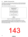
3. tOPW is defined by the value given in figure 6-4, High-Speed, High-Reliability
Programming Flow Chart.
125

 ETC [ ETC ]