Si3210/Si3211/Si3212
Electrical Specifications
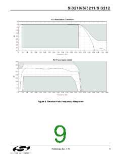
*
Table 1. Absolute Maximum Ratings and Thermal Information
Parameter
Symbol
, V , V
DDA2
Value
–0.5 to 6.0
±10
Unit
V
DC Supply Voltage
V
DDD
DDA1
Input Current, Digital Input Pins
Digital Input Voltage
I
mA
V
IN
V
–0.3 to (VDDD + 0.3)
2000
IND
ESD, Si3210/11/12 (Human Body Model)
Operating Temperature Range
Storage Temperature Range
V
T
–40 to 100
–40 to 150
50
°C
A
T
°C
STG
TSSOP-38 Thermal Resistance, Typical
θ
°C/W
JA
*Note: Permanent device damage may occur if the above Absolute Maximum Ratings are exceeded. Functional operation
should be restricted to the conditions as specified in the operational sections of this data sheet. Exposure to absolute
maximum rating conditions for extended periods may affect device reliability.
Table 2. Recommended Operating Conditions
Test
Parameter
Symbol
Min*
Typ
Max*
Unit
Condition
o
Ambient Temperature
T
K-grade
B-grade
0
25
25
70
85
C
A
o
Ambient Temperature
T
–40
3.13
C
A
Si3210/11/12 Supply Voltage
V
,V
3.3/5.0
5.25
V
DDD DDA1
,V
DDA2
*Note: All minimum and maximum specifications are guaranteed and apply across the recommended operating conditions.
o
Typical values apply at nominal supply voltages and an operating temperature of 25 C unless otherwise stated.
Product specifications are only guaranteed when the typical application circuit (including component tolerances) is
used.
4
Preliminary Rev. 1.11

 ETC [ ETC ]