PRELIMINARY
PCT1789W DATA SHEET
!!
FIGURES
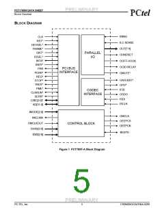
Figure 1 PCT789 Block Diagram . . . . . . . . . . . . . . . . 5
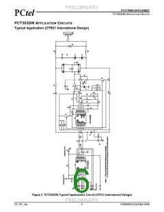
Figure 2 PCT303DW Typical Applications Circuit
Figure 18 Serial Interface Timing Diagram (DCE = 1,
FSD = 0). . . . . . . . . . . . . . . . . . . . . . . . . . . . . . . . . 56
Figure 19 Serial Interface Timing Diagram (DCE = 1,
FSD = 1). . . . . . . . . . . . . . . . . . . . . . . . . . . . . . . . . 57
Figure 20 Test Circuit For Loop Characteristics . . . . 58
Figure 21 FIR Receive Filter Response . . . . . . . . . . 59
Figure 22 FIR Receive Filter Passband Ripple. . . . . 59
Figure 23 FIR Transmit Filter Response. . . . . . . . . . 59
Figure 24 FIR Transmit Filter Passband Ripple . . . . 59
Figure 25 IIR Receive Filter Response. . . . . . . . . . . 60
Figure 26 IIR Receive Filter Passband Ripple . . . . . 60
Figure 27 IIR Transmit Filter Response . . . . . . . . . . 60
Figure 28 IIR Transmit Filter Passband Ripple. . . . . 60
Figure 29 IIR Receive Group Delay . . . . . . . . . . . . . 60
Figure 30 IIR Transmit Group Delay. . . . . . . . . . . . . 60
Figure 31 100-Pin TQFP Package . . . . . . . . . . . . . . 61
Figure 32 16-pin SOIC Package. . . . . . . . . . . . . . . . 62
Figure 33 Mode 0 I/V Characteristics (0,0). . . . . . . . 63
Figure34TypicalApplicationsCircuit(NET4Specifications)
64
(CRT21 International Design) . . . . . . . . . . . . . . . . . 6
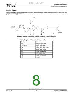
Figure 3 Optional Connection to AOUT For a Call
Progress Speaker . . . . . . . . . . . . . . . . . . . . . . . . . . 8
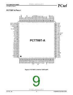
Figure 4 PCT789T 100-Pin TQFP/LQFP. . . . . . . . . . 9
Figure 5 PCT303D 16-Pin SOIC . . . . . . . . . . . . . . . 14
Figure 6 PCT303W 16-Pin SOIC. . . . . . . . . . . . . . . 14
Figure 7 Mode 1 I/V Characteristics (0,1) . . . . . . . . 17
Figure 8 Mode 2 I/V Characteristics (1,0) . . . . . . . . 18
Figure 9 Mode 3 I/V Characteristics (1,1) . . . . . . . . 18
Figure 10 Ring Detect Timing . . . . . . . . . . . . . . . . . 19
Figure 11 Software FC/RGDT Secondary Request . 20
Figure 12 Hardware FC/RGDT Secondary Request 21
Figure 13 Secondary Communication Data Format -
Read Cycle . . . . . . . . . . . . . . . . . . . . . . . . . . . . . . 21
Figure 14 Secondary Communication Data Format -
Write Cycle . . . . . . . . . . . . . . . . . . . . . . . . . . . . . . 22
Figure 15 Clock Generation Subsystem . . . . . . . . . 23
Figure 16 General Inputs Timing Diagram. . . . . . . . 54
Figure 17 Serial Interface Timing Diagram (DCE = 0)55
TABLES
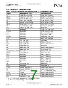
Table 1 PCT303DW Typical Application Component
Values (CTR21 International Design) . . . . . . . . . . . 7
Table 2 Optional Connection Component Values . . . 8
Table 3 PCT789A Pin Description . . . . . . . . . . . . . . 10
Table 4 PCT789A Operating Mode Configuration . . 13
Table 5 PCT303D Pin Description. . . . . . . . . . . . . . 15
Table 6 PCT303W Pin Descriptions . . . . . . . . . . . . 16
Table 7 PCT301L/PCT303W Pin Comparison. . . . . 16
Table 8 Line Interface Configurations (Register 16) 18
Table 9 Serial Modes. . . . . . . . . . . . . . . . . . . . . . . . 19
Table 10 N2, M2 Values (CGM = 0, 1). . . . . . . . . . . 22
Table 11 MCLK Examples . . . . . . . . . . . . . . . . . . . . 24
Table 12 Revision Values . . . . . . . . . . . . . . . . . . . . 26
Table 13 PCT789A Base I/O Definition . . . . . . . . . . 28
Table 14 PCI Configuration Registers . . . . . . . . . . . 29
Table 15 PCT789A Control Registers . . . . . . . . . . . 36
Table 16 PCT789A Absolute Maximum Ratings . . . 49
Table 17 PCT789A DC Characteristics . . . . . . . . . . 49
Table 20 PCT303DW Loop Characteristics . . . . . . . 51
Table 21 PCT303DW DC Characteristics, VD = +5V 51
Table 22 PCT303DW DC Characteristics, VD = +3.3V
52
Table 23 PCT303DW AC Characteristics. . . . . . . . . 53
Table 24 Switching Characteristics—General Inputs 54
Table 25 Switching Characteristics—Serial Interface
(DCE = 0) . . . . . . . . . . . . . . . . . . . . . . . . . . . . . . . . 55
Table 26 Switching Characteristics—Serial Interface
(DCE = 1, FSD = 0) . . . . . . . . . . . . . . . . . . . . . . . . 56
Table 27 Switching Characteristics—Serial Interface
(DCE = 1, FSD = 0) . . . . . . . . . . . . . . . . . . . . . . . . 57
Table 28 Digital FIR Filter Characteristics—Transmit
and Receive . . . . . . . . . . . . . . . . . . . . . . . . . . . . . . 58
Table 29 Digital IIR Filter Characteristics—Transmit and
Receive . . . . . . . . . . . . . . . . . . . . . . . . . . . . . . . . . 58
Table 30 TQFP Mechanical Dimensions . . . . . . . . . 61
Table 31 SOIC Mechanical Dimensions. . . . . . . . . . 62
Table18PCT303DWRecommendedOperatingConditions Table 32 Component Values (NET4 Specifications) 65
50
Table 33 NET4 Country Line Interface Configurations
(Register 16) . . . . . . . . . . . . . . . . . . . . . . . . . . . . . 67
Table 19 PCT303DW Absolute Maximum Ratings . 50
PRELIMINARY
PC-TEL, Inc.
4
1789W0DOCDAT06A-0299

 ETC [ ETC ]