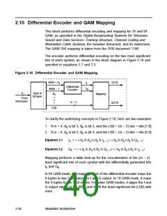
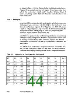
As shown in Figure 2.18, the filter shifts four coefficient register banks
(Register 0) sequentially, starting with register 48 and proceeding down
to 0. In this configuration, it shifts bank 3 first, then 49 bytes of bank 2,
bank 1, and, finally, bank 0. Table 2.1 shows the exact allocation of bits
within each bank.
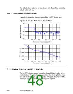
2.11.2 Example
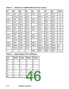
Assuming all filter configuration bits are located in a host microprocessor
ROM array of bytes addressed with [0 to 195], the filter coefficients place
phase 0 coefficients in registers [0 to 48], phase 1 in [49 to 97], phase
2 in [98 to 146], and phase 3 in [147 to 195]. To download this array, the
microprocessor must write bytes [195 down to 0] sequentially into
address 0 register, highest array address first.
After 196 write cycles, the four coefficient register banks are completely
configured. During configuration, the filter is not operational to save gates
by avoiding double buffering of the coefficient registers. For different
QAM modes, the filter must load the appropriate sets of coefficients and
shifter values.
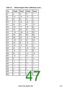
The default set of coefficients is a square-root raised cosine filter. The
filter sets the coefficients in Table 2.2 after reset, and it can overwrite
2
them with external programming through the I C-compatible interface.
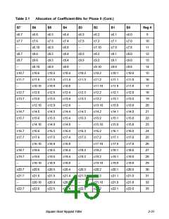
Table 2.1
B7
Allocation of Coefficient-Bits for Phase 0
B6
B5
B4
B3
B2
B1
B0
Reg #
c0.7
c1.7
–
c0.6
c1.6
c0.10
c2.6
c3.6
c2.10
c4.6
c5.6
c4.10
c0.5
c1.5
c0.9
c2.5
c3.5
c2.9
c4.5
c5.5
c4.9
c0.4
c1.4
c0.8
c2.4
c3.4
c2.8
c4.4
c5.4
c4.8
c0.3
c1.3
–
c0.2
c1.2
c1.10
c2.2
c3.2
c3.10
c4.2
c5.2
c5.10
c0.1
c1.1
c1.9
c2.1
c3.1
c3.9
c4.1
c5.1
c5.9
c0.0
c1.0
c1.8
c2.0
c3.0
c3.8
c4.0
c5.0
c5.8
0
1
2
3
4
5
6
7
8
c2.7
c3.7
–
c2.3
c3.3
–
c4.7
c5.7
–
c4.3
c5.3
–
2-30
Modulator Architecture

 ETC [ ETC ]