Version: 1.18
PRELIMINARY/CONFIDENTIAL
TrueSpeech® Co-Processor
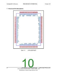
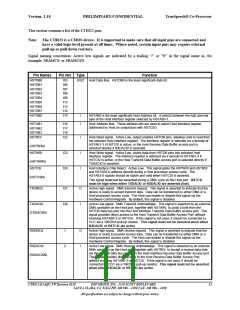
Pin Names
Pin Nrs
Type
Function
GPIO0,
DATAFLAG\
4
I/O
General-purpose
pins.
input/output
For CT8015 compatibility:
GPIO 0 may be assigned as DATAFLAG\ (output)
GPIO1
GPIO2
GPIO3
GPIO4
5
6
7
8
GPIO 5 may be assigned as Frame Interrupt, FR\ (output)
After and during reset, all the GPIO pins are all configured as inputs. (Compatibility
Note: the CT8020 configures GPIO0 and 5 as outputs by default)
Connect 47K ohm pull-down resistors to GND on each GPIO pin to ensure that a
valid input signal level is present at all times.
GPIO5, FR\
9
GPIO6
GPIO7
12
13
SCLK
34
I/O
I/O
Shift Clock for CODEC interface. During and after reset, this pin is configured as an
input. Connect 47K ohm pull-down resistors to GND to this pin to ensure that a
valid input signal level is present at all times. If an external signal permanently
drives this pin, no pull-down is required. The SCLK signal is typically expected to
operate at 2.048 MHz. When used as an output (master mode) the SCLK rate is
programmable by the Host.
Frame Sync clock for CODEC interface. During and after reset, this pin is configured
as an input. Connect 47K ohm pull-down resistors to GND to this pin to ensure
that a valid input signal level is present at all times. If an external signal
permanently drives this pin, no pull-down is required. The FSYNC signal is typically
expected to operate at 8 KHz to provide the 8KHz sample clock required by the
external serial CODEC. When used as an output (master mode), the FSYNC rate is
programmable by the Host.
FSYNC
35
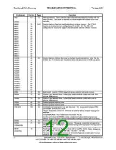
DX0
DR0
30
31
O/Z
I
Serial Transmit Data Output for CODEC 0. This output is always high impedance
when not transmitting data. This CODEC pin is used for telephone line output in
Standalone Speakerphone mode.
Serial Receive Data Input for CODEC 0. Connect 47K ohm pull-down resistors to
GND to this pin to ensure that a valid input signal level is present at all times.
Note that CODEC chip output pins typically tri-state when not actually transmitting
data. This CODEC pin is used for telephone line input in Standalone Speakerphone
mode.
DX1
DR1
32
33
O/Z
I
Serial Transmit Data Output for CODEC 1. This output is always high impedance
when not transmitting data. This is the default CODEC output used for playback.
Serial Receive Data Input for CODEC 1 Connect 47K ohm pull-down resistors to
GND to this pin to ensure that a valid input signal level is present at all times.
Note that CODEC chip output pins typically tri-state when not actually transmitting
data. This is the default CODEC input used for record.
XIN
XOUT
CLKOUT
22
23
17
I
O
O
Crystal Input or external oscillator input.
Crystal Output
Clock Out = MAINCLOCK/(CLK_RATE+1). This is the internal CT8022 DSP core
clock. It is possible to disable the output reduce power consumption.
The MAINCLOCK frequency in PLL mode, is the external crystal frequency * 11.
In PLL by-pass mode, MAINCLOCK is the external oscillator frequency divided by 2.
CLK_RATE is the DSP core clock division factor that the Host controller may program
using the slow down mode command.
Note that significant short-term clock jitter may be present on the CLKOUT signal
when the PLL is enabled.
TEST
PLLR
PLLC
PLLT
AVCC(VCC3)
AGND(GND3)
PLLBYPASS
15
24
25
26
21
27
18
I
Reserved - connect to GND.
Analog PLL support circuitry pins. Connect to external PLL filter circuit.
Analog
Analog PLL VCC connection
Power PLL GND connection
Power
I
Disables internal PLL when high and allows direct use of an external (90.112 MHz)
clock applied to the XIN pin. Connect to GND when operating using PLL and external
4.096 MHz crystal.
CT8022A11AQC FW Revision 0118 DSP GROUP, INC., 3120 SCOTT BOULEVARD
SANTA CLARA, CA 95054 PH: 408 986 – 4300 FAX: 408 986 – 4490
13
All specifications are subject to change without prior notice.

 ETC [ ETC ]