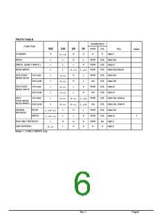
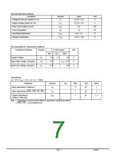
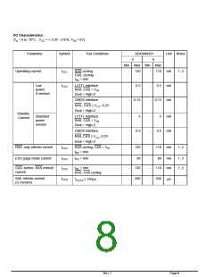
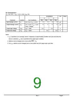
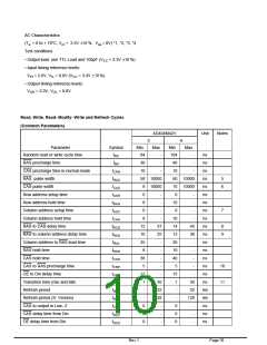
AC Characteristics
(Ta = 0 to + 70°C, Vcc = 3.3V ±10 %, Vss = 0V) *1, *2, *3, *4
Test conditions
• Output load: one TTL Load and 100pF (VCC = 3.3V ±10 %)
• Input timing reference levels:
VIH = 2.0V, VIL = 0.8V (VCC = 3.3V ±10 %)
• Output timing reference levels:
VOH = 2.0V, VOL = 0.8V
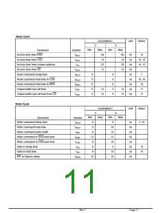
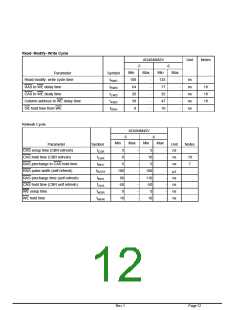
Read, Write, Read- Modify- Write and Refresh Cycles
(Common Parameters)
AD404M42V
Unit
Notes
-5
-6
Parameter
Symbol
tRC
Min
84
Max
Min
104
Max
Random read or write cycle time
-
-
-
-
-
-
ns
ns
ns
ns
ns
ns
ns
ns
ns
ns
ns
ns
ns
ns
ns
ns
ns
ms
ms
ns
ns
ns
RAS precharge time
tRP
tCPN
tRAS
tCAS
tASR
tRAH
tASC
tCAH
tRCD
tRAD
tRAL
tRSH
tCSH
tCRP
tOED
tT
30
10
40
10
CAS precharge time in normal mode
RAS pulse width
50 10000
60 10000
10 10000
5
6
CAS pulse width
8
0
10000
Row address setup time
Row address hold time
Column address setup time
Column address hold time
RAS to CAS delay time
RAS to column address delay time
Column address to RAS lead time
RAS hold time
-
0
10
0
-
8
-
-
0
-
-
7
8
-
10
14
12
30
10
40
5
-
12
10
25
8
37
45
8
9
25
30
-
-
-
-
CAS hold time
38
5
-
-
CAS to RAS precharge time
OE to Din delay time
-
-
10
11
12
1
-
50
32
128
-
15
1
-
50
32
128
-
Transition time (rise and fall)
Refresh period
tREF
tREF
tCLZ
tDZC
tDZO
-
-
Refresh period (S- Version)
CAS to output in Low- Z
CAS delay time from Din
OE delay time from Din
-
-
0
0
0
-
0
-
0
-
0
-
Rev.1
Page10

 ETC [ ETC ]