2N60
Power MOSFET
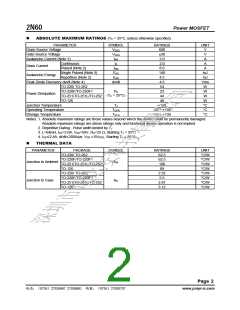
ELECTRICAL CHARACTERISTICS (TJ =25°С, unless otherwise specified)
PARAMETER
SYMBOL
TEST CONDITIONS
MIN TYP MAX UNIT
OFF CHARACTERISTICS
Drain-Source Breakdown Voltage
Drain-Source Leakage Current
BVDSS
IDSS
VGS = 0V, ID = 250μA
600
V
VDS = 600V, VGS = 0V
10
μA
Forward
Reverse
V
GS = 30V, VDS = 0V
100 nA
-100 nA
V/°С
Gate-Source Leakage Current
IGSS
VGS = -30V, VDS = 0V
Breakdown Voltage Temperature Coefficient △BVDSS/△TJ ID=250μA, Referenced to 25°C
0.4
3.6
ON CHARACTERISTICS
Gate Threshold Voltage
VGS(TH)
RDS(ON)
VDS = VGS, ID = 250μA
2.0
4.0
5
V
Static Drain-Source On-State Resistance
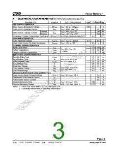
DYNAMIC CHARACTERISTICS
Input Capacitance
VGS = 10V, ID =1A
Ω
CISS
COSS
CRSS
270 350 pF
V
DS =25V, VGS =0V,
Output Capacitance
40
5
50
7
pF
pF
f =1MHz
Reverse Transfer Capacitance
SWITCHING CHARACTERISTICS
Turn-On Delay Time
tD (ON)
tR
tD(OFF)
tF
10
25
30
60
50
60
11
ns
ns
Turn-On Rise Time
VDD =300V, ID =2.4A,
RG=25Ω (Note 1, 2)
Turn-Off Delay Time
20
ns
Turn-Off Fall Time
25
ns
Total Gate Charge
QG
9.0
1.6
4.3
nC
nC
nC
VDS=480V, VGS=10V,
ID=2.4A (Note 1, 2)
Gate-Source Charge
QGS
QGD
Gate-Drain Charge
DRAIN-SOURCE DIODE CHARACTERISTICS
Drain-Source Diode Forward Voltage
Continuous Drain-Source Current
Pulsed Drain-Source Current
Reverse Recovery Time
VSD
ISD
ISM
trr
VGS = 0 V, ISD = 2.0 A
1.4
2.0
8.0
V
A
A
180
ns
μC
V
GS = 0 V, ISD = 2.4A,
di/dt = 100 A/μs (Note 1)
Reverse Recovery Charge
QRR
0.72
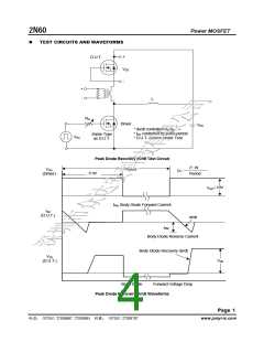
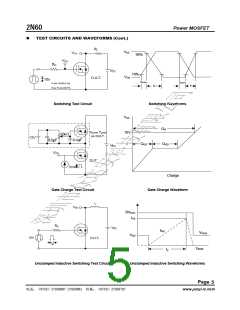
Notes: 1. Pulse Test: Pulse width ≤ 300μs, Duty cycle≤2%
2. Essentially independent of operating temperature
深圳市众达安科技有限公司
Page 3
:(0755)27858667 27858661
真:(0755)27858707
www.junyi-ic.com

 ETC [ ETC ]