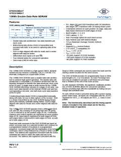
NT5DS32M4AT
NT5DS16M8AT
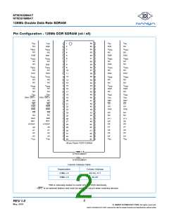
128Mb Double Data Rate SDRAM
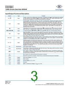
Input/Output Functional Description
Symbol
CK, CK
Type
Input
Function
Clock: CK and CK are differential clock inputs. All address and control input signals are sampled
on the crossing of the positive edge of CK and negative edge of CK. Output (read) data is refer-
enced to the crossings of CK and CK (both directions of crossing).
Clock Enable: CKE HIGH activates, and CKE Low deactivates, internal clock signals and device
input buffers and output drivers. Taking CKE Low provides Precharge Power-Down and Self
Refresh operation (all banks idle), or Active Power-Down (row Active in any bank). CKE is syn-
chronous for power down entry and exit, and for self refresh entry. CKE is asynchronous for self
refresh exit. CKE must be maintained high throughout read and write accesses. Input buffers,
excluding CK, CK and CKE are disabled during power-down. Input buffers, excluding CKE, are
disabled during self refresh.
CKE
Input
Chip Select: All commands are masked when CS is registered high. CS provides for external
bank selection on systems with multiple banks. CS is considered part of the command code.
CS
Input
Input
RAS, CAS, WE
Command Inputs: RAS, CAS and WE (along with CS) define the command being entered.
Input Data Mask: DM is an input mask signal for write data. Input data is masked when DM is
sampled high coincident with that input data during a Write access. DM is sampled on both edges
of DQS. Although DM pins are input only, the DM loading matches the DQ and DQS loading.Dur-
ing a Read, DM can be driven high, low, or floated.
DM
Input
Input
Bank Address Inputs: BA0 and BA1 define to which bank an Active, Read, Write or Precharge
command is being applied. BA0 and BA1 also determines if the mode register or extended mode
register is to be accessed during a MRS or EMRS cycle.
BA0, BA1
Address Inputs: Provide the row address for Active commands, and the column address and
Auto Precharge bit for Read/Write commands, to select one location out of the memory array in
the respective bank. A10 is sampled during a Precharge command to determine whether the Pre-
charge applies to one bank (A10 low) or all banks (A10 high). If only one bank is to be precharged,
the bank is selected by BA0, BA1. The address inputs also provide the op-code during a Mode
Register Set command.
A0 - A11
Input
DQ
Input/Output
Input/Output
Data Input/Output: Data bus.
Data Strobe: Output with read data, input with write data. Edge-aligned with read data, centered
in write data. Used to capture write data.
DQS
FET control: Optional. Output during every Read and Write access. Is provided to control isola-
QFC
Output
tion switches on modules. Open drain output. Pullup resistor connected to V
at second level of assembly.
must be supplied
DDQ
NC
No Connect: No internal electrical connection is present.
DNU
Electrical connection is present. Should not be connected at second level of assembly.
V
Supply
Supply
Supply
Supply
Supply
DQ Power Supply: 2.5V ± 0.2V.
DQ Ground
DDQ
V
SSQ
V
Power Supply: 2.5V ± 0.2V.
Ground
DD
V
SS
V
SSTL_2 reference voltage: (V
/ 2) ± 1%.
DDQ
REF
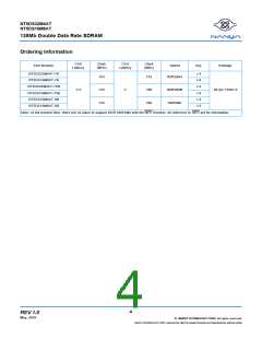
3
REV 1.0
May, 2001
©
NANYA TECHNOLOGY CORP. All rights reserved.
NANYA TECHNOLOGY CORP. reserves the right to change Products and Specifications without notice.

 ETC [ ETC ]