ZENTRUM MIKROELEKTRONIK DRESDEN AG
“ASI for you” IC
Datasheet
3.17 Power Supply
The power supply block provides a sensor supply, which is inductively decoupled from the AS-i bus voltage, at
pin UOUT. The decoupling is realized by an electronic inductor circuit, which basically consists of a current
source and a controlling low pass. The time constant of the low pass, that has influence to the resulting input
impedance at pin UIN, can be adjusted by an external capacitor at pin CAP.
The electronic inductor can be turned off if pin CAP is connected to 0V. This shuts down the current source
between UIN and UOUT requiring an external connection between UIN and UOUT for proper IC operation. The
possibility to turn off the electronic inductor is helpful to realize high symmetrical extended power applications
(i.e. AS-i connected actuators with large load currents).
Overloading the electronic inductor for more than 2 seconds by drawing too much current shuts down the entire
IC in order to avoid a deviation of the input impedance, which would have negative influence to the communica-
tion of the remaining AS-i network clients. The fail-safe shutdown mode can only be left by power cycling the
AS-i supply voltage.
A second function of the power supply block is to generate a regulated 5V supply for operation of the internal
logic and some analog circuitry. The voltage is provided at pin U5R an can be used to supply external circuitry
as well, as long as the current requirements stay within in the specified limits. See Table 33 below. Because the
5V supply is generated out of the decoupled sensor supply at UOUT, the current drawn at U5R has to be sub-
tracted from the total available load current at UOUT.
The power supply dissipates the major amount of power:
Ptot = VDrop* IUOUT + (VUOUT-5V) * I5V
In total, the power dissipation shall not exceed the specified values of chapter 1.1.
To cope with fast internal and external load changes (spikes) external capacitors at UOUT and U5R are re-
quired. The 0V pin defines the ground reference voltage for both UOUT and U5R.
3.17.1 Voltage Output Pins UOUT and U5R
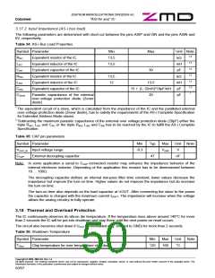
Table 33: Properties of voltage output pins UOUT and U5R
Symbol Parameter
Min
16
Max
33.1
6.7 2
Unit
V
Note
1
VUIN
Positive supply voltage for IC operation
VDROP
VUOUT
Voltage drop from pin UIN to pin UOUT
UOUT output supply voltage
5.5 2
V
VUIN > 22V
VUIN- VDROPmax VUIN- VDROPmin
V
IUOUTmax
2
VUOUTp UOUT output voltage pulse deviation
1.5
2
V
2
tUOUTp
UOUT output voltage pulse deviation
width
ms
VU5R
IUOUT
I5V
5V supply voltage
4.5
0
5.5
55 2
4
V
UOUT output supply current
U5R output supply current
Total output current IUOUT + I5V
Short circuit output current
mA
mA
mA
mA
µF
IU5R = 0 2
0
Io
55
IUOUTS
50
10
1
CBUOUT Blocking capacitance at UOUT
CB5V Blocking capacitance at U5R
470
µF
1 Parameter copied from Table 2: Operating Conditions
2 CUOUT = 10µF, output current switches from 0 to IUOUTmax and vice versa
Copyright © 2006, ZMD AG, Rev.1.4
All rights reserved. The material contained herein may not be reproduced, adapted, merged, translated, stored, or used without the prior written consent of the copyright owner. The
Information furnished in this publication is preliminary and subject to changes without notice.
49/57

 ZMD [ Zentrum Mikroelektronik Dresden AG ]