ZNBG3113
ZNBG3114
APPLICATIONS INFORMATION(cont)
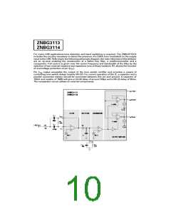
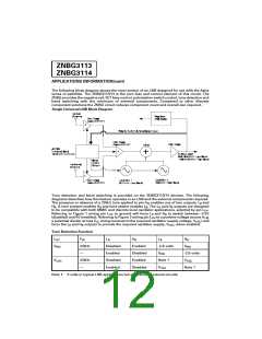
The following block diagram shows the main section of an LNB designed for use with the Astra
series of satellites. The ZNBG3113/14 is the core bias and control element of this circuit. The
ZNBG provides the negative rail, FET bias control, polarisation switch control, tone detection and
band switching with the minimum of external components. Compared to other discrete
component solutions the ZNBG circuit reduces component count and overall size required.
Single Universal LNB Block Diagram
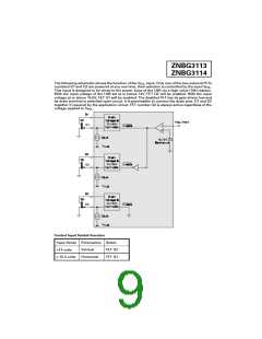
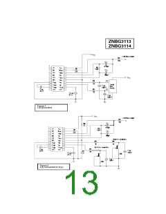
Tone detection and band switching is provided on the ZNBG3113/14 devices. The following
diagrams describes how this feature operates in an LNB and the external components required.
The presence or absence of a 22kHz tone applied to pin FIN enables one of two outputs, LB and
HB. A tone present enables HB and tone absent enables LB. The LB and HB outputs are designed
to be compatible with both MMIC and discrete local oscillator applications, selected by pin LOV
.
Referring to Figure 1 wiring pin LOV to ground will force LB and HB to switch between -2.6V
(disabled) and 0V (enabled). Referring to Figure 2 wiring pin LOV to a positive voltage source (e.g.
a potential divider across VCC and ground set to the required oscillator supply voltage, VOSC) will
force the LB and HB outputs to provide the required oscillator supply, VOSC, when enabled.
Tone Detection Function
LOV
FIN
LB
HB
LB
HB
GND
22kHz
—
Disabled
Enabled
Disabled
Enabled
Enabled
Disabled
Enabled
Disabled
-2.6 volts
GND
GND
-2.6 volts
VOSC
VOSC
22kHz
—
Note 1
VOSC
Note 1
Note 1: 0 volts in typical LNB applications but ependent on extenal circuits.
4-134

 ZETEX [ ZETEX SEMICONDUCTORS ]