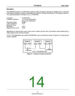
MT88E45
Data Sheet
1.00
0.95
0.90
0.85
0.80
0.75
0.70
0.65
0.60
0.55
0.50
Gain ratio for
Bellcore GS1, GS2
ETSI GS2 op amps
0.794
Gain ratio for ETSI
GS1 op amp
0.668
0.531
3.0
3.5
4.0
Nominal Vdd (Volts)
4.5
5.0
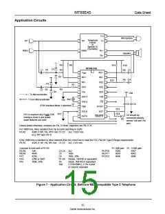
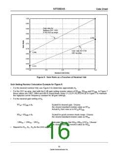
Figure 8 - Gain Ratio as a Function of Nominal Vdd
Gain Setting Resistor Calculation Example for Figure 8:
•
•
For the desired nominal Vdd, use Figure 8 to determine approximate Av.
For the GS1 op-amp, start with the 0 dB gain setting resistor values of R50dB, R60dB and R70dB. In Figure 7
these values are 53K7, 60K4 and 464 K respectively. Keep C1,C2,R1,R2,R3,R4 as in Figure 7 to maintain
the highpass corner frequency constant for all gain settings.
•
For the desired gain setting of Av:
R7Av= R70dB x AV
R5Av= R50dB x AV
Scaled for desired gain. Choose
the closest standard resistor value as R7Av.
Actual Av from now on is R7Av/R70db
Scaled for good common mode range. Choose
the closest standard resistor value as R5Av.
1/R6Av = 1/R5Av - 1/R7Av
Calculate R6Av so that R5Av=R6Av || R7Av. Choose
the closest standard resistor value as R6Av.
•
Repeat for R10, R11, R12 for the GS2 op-amp.
16
Zarlink Semiconductor Inc.

 ZARLINK [ ZARLINK SEMICONDUCTOR INC ]