MT88E45
Data Sheet
If DCLK begins while DR is low, DR will return to high upon the first DCLK rising edge. If DR interrupts a
microcontroller then this feature allows the interrupt to be cleared by the first read pulse. Otherwise DR is low for
half a nominal bit time (1/2400 sec).
Reading the stop bit allows the software to check for framing errors. When framing error is not checked the
microcontroller only needs to send 8 DCLK pulses to shift the data byte out.
Carrier Detect
The carrier detector provides an indication of the presence of a signal in the FSK frequency band. It detects the
presence of a signal of sufficient amplitude at the output of the FSK bandpass filter. The signal is qualified by a
frequency aware digital algorithm before the CD output is set low to indicate carrier detection. A 10 ms hysteresis is
provided to allow for momentary signal dropout once CD has been activated. CD is released when there is no
activity at the FSK bandpass filter output for 10 ms.
When CD is inactive (high), the raw output of the FSK demodulator is ignored by the internal data timing recovery
circuit. In mode 0 the DATA, DCLK and DR pins are forced high. In mode 1 the output shift register is not updated
and DR is high; if DCLK is clocked, DATA is undefined.
Note that signals such as speech, CAS and DTMF tones also lie in the FSK frequency band and the carrier detector
may be activated by these signals. They will be demodulated and presented as data. To avoid the false data, the
MT88E45B should be put into CAS or power down mode when FSK is not expected. Ringing, on the other hand,
does not pose a problem as it is ignored by the carrier detector.
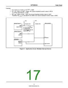
Interrupt
The DR/STD output can be used to interrupt a microcontroller. When the MT88E45B is the only interrupt source,
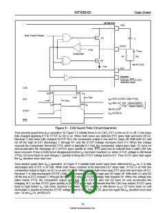
DR/STD can be connected directly to the microcontroller’s interrupt input. Figure 9 shows the necessary
connections when the MT88E45B is one of many interrupt sources. The diodes and resistors implement a wired-or
so that the microcontroller is interrupted (INT low active or falling edge triggered) when one or more of INT1, INT2
or DR/STD is low. The microcontroller can determine which one of DR/STD, INT1 or INT2 caused the interrupt by
reading them into an input port.
When system power is first applied and CB0/1/2 have already been configured to select CAS detection, DR/STD
will power up as logic low. This is because there is no charge across the ST/GT capacitor in Figure 55, hence
ST/GT is at Vdd which causes STD to be low. If DR/STD is used to interrupt a microcontroller the interrupt will not
clear until the capacitor has charged up. Therefore upon initial power up the microcontroller should ignore this
interrupt source until there is sufficient time to charge the capacitor. Alternatively, the MT88E45B can be put into
power down mode: DR/STD goes high and clears the interrupt, ST/GT goes low and the capacitor will charge up
quickly.
Power Down
The MT88E45B can be powered down to consume virtually no power supply current via a state of the CB0/1/2 pins.
Momentary transition of CB0/1/2 into the power down code will not activate power down.
In power down mode both input op-amps, VREF and the oscillator are non functional. DCLK becomes an input
because to select the power down state CB0 is 1 which will select FSK interface mode 1. If the application uses
FSK interface mode 0 and the MT88E45B needs to be powered down then a pull down resistor should be added
at the DCLK pin to define its state during power down (R15 in Figure 7). When the MT88E45B is powered down
DATA, DR/STD, CD are high; EST and ST/GT are low.
To reduce the operating current an Intelligent Power Down feature has been incorporated. When FSK is selected,
the CAS detector is powered down. When CAS is selected the FSK demodulator is powered down. The two input
op-amps are not affected and both will remain operational.
13
Zarlink Semiconductor Inc.

 ZARLINK [ ZARLINK SEMICONDUCTOR INC ]