MT88E43B
Data Sheet
24
23
22
21
20
19
18
17
16
15
14
13
1
2
IN+
IN-
VDD
St/GT
ESt
GS
3
4
5
StD
VRef
CAP
INT
TRIGin
6
7
CD
TRIGRC
DR
8
DATA
DCLK
FSKen
PWDN
IC
TRIGout
MODE
OSCin
OSCout
VSS
9
10
11
12
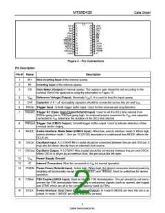
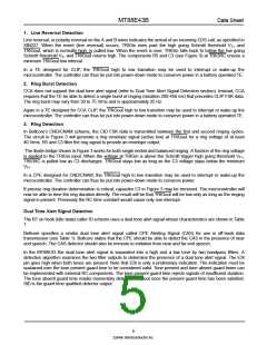
Figure 2 - Pin Connections
Pin Description
Pin # Name
Description
1
2
3
IN+
IN-
GS
Non-inverting Input of the internal opamp.
Inverting Input of the internal opamp.
Gain Select (Output) of internal opamp. The opamp’s gain should be set according to the
nominal Vdd of the application using the information in Figure 10.
4
5
6
7
VRef
Reference Voltage (Output). Nominally VDD/2. It is used to bias the input opamp.
CAP Capacitor. A 0.1 µF decoupling capacitor should be connected across this pin and VSS.
TRIGin Trigger Input. Schmitt trigger buffer input. Used for line reversal and ring detection.
TRIGRC Trigger RC (Open Drain Output/Schmitt Input). Used to set the (RC) time interval from
TRIGin going low to TRIGout going high. An external resistor connected to VDD and capacitor
connected to VSS determine the duration of the (RC) time interval.
8
9
TRIGout Trigger Out (CMOS Output). Schmitt trigger buffer output. Used to indicate detection of line
reversal and/or ringing.
MODE 3-wire interface: Mode Select (CMOS Input). When low, selects interface mode 0. When high,
selects interface mode 1. See pin 16 (DCLK) description to understand how MODE affects the
DCLK pin.
10
11
OSCin Oscillator Input. A 3.579545 MHz crystal should be connected between this pin and OSCout. It
may also be driven directly from an external clock source.
OSCout Oscillator Output. A 3.579545 MHz crystal should be connected between this pin and OSCin.
When OSCin is driven by an external clock, this pin should be left open.
12
13
14
VSS
IC
Power Supply Ground.
Internal Connection. Must be connected to VSS for normal operation.
PWDN Power Down (Schmitt Input). Active high. When high, the device consumes minimal power by
disabling all functionality except TRIGin, TRIGRC and TRIGout. Must be pulled low for device
operation.
15
16
FSKen FSK Enable (CMOS Input). Must be high for FSK demodulation. This pin should be set low to
prevent the FSK demodulator from reacting to extraneous signals (such as speech, alert signal
and DTMF which are all in the same frequency band as FSK).
DCLK 3-wire Interface: Data Clock (CMOS Input/Output). In mode 0 (MODE pin low), this pin is an
output. In mode 1 (MODE pin high), this pin is an input.
2
Zarlink Semiconductor Inc.

 ZARLINK [ ZARLINK SEMICONDUCTOR INC ]