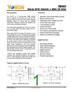
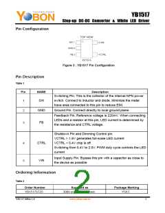
YB1517
Step-up DC-DC Converter & White LED Driver
Absolute Maximum Ratings
Recommended Operating Conditions
Operating Temperature (note 3) .........................-40°C~85°C
VIN.................................................................................20V
SW Voltage ....................................................................35V Supply Voltage .................................................... 2.7 V~16V
FB Voltage .......................................................................5V SW Voltage ....................................................................30V
CTRL Voltage...................................................................5V ESD Susceptibility (HBM).............................................. 2KV
Maximum Junction Temp,TJ (not 2) ............................150°C
Lead Temperature (Soldering 10 sec).........................250°C
Thermal Resistance (SOT-25, θJA).......................250℃/W
Internal Power Disspation (SOT-25, PD)......................0.4W
ESD Susceptibility (MM)...............................................200V
Electricity Characteristics
(TA=25°C, Vin=3.3V, L=22uH, Cin=1uF, Cout=4.7uF unless otherwise noted)
Table 3
Symbol
Function Parameter
Input Voltage Range
Not Switching
Test Conditions
Min
2.7
Typ
Max
16
Units
V
Vin
IQ
VFB = 0.5V
CTRL = 0V
1.2
1.5
0.3
1.7
mA
(Quiescent
Current)
Shutdown
1
uA
Iout=20mA,Vout = 6V
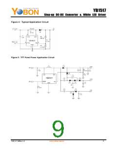
Circuit of Figure 2
VFB
Feedback Voltage
210
850
220
230
mV
100% duty cycle
40% duty cycle
VFB=220mV
900
400
1000
mA
mA
ICL
Switch Current Limit
IB
FB Pin Bias Current
Switching Frequency
1
uA
FRSW
850
20
900
950
KHz
DTMX
DTMN
VSAT
Maximum Duty Cycle
Minimum duty cycle
Switch Vcesat
85
25
%
%
At Isw = 200mA
Ctrl = 0.5V
180
mV
ILKG
Switch Leakage Current
1
μA
VCTRL for Full LED
current
Full On
Full Off
1.7
V
V
VCTL
0.3
ICTL
OVP
θJA
CTRL Pin Bias Current
Over Voltage Protection
Thermal Resistance
Ctrl = 2V
40
34
μA
V
220
°C/W
Note:
Absolute maximum ratings are limits beyond which damage to the device may occur. The maximum
allowable, power dissipation at any ambient temperature is calculated using: PD(MAX)= [TJ(max)-TA]/θJA .
YB1517 MRev.1.0
www.yobon.com.tw
3

 YOBON [ YOBON TECHNOLOGIES,INC. ]