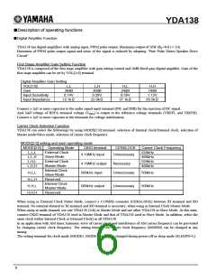
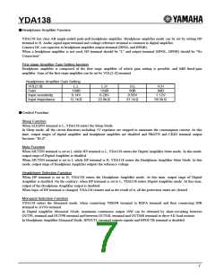
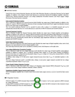
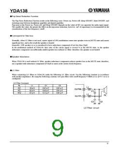
YDA138
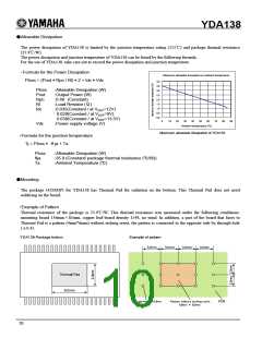
●Allowable Dissipation
The power dissipation of YDA138 is limited by the junction temperature rating (125℃) and package thermal resistance
(35.9℃/W).
The power dissipation and junction temperature of YDA138 can be found by the following formula.
For the use of YDA138, take care not to exceed the power dissipation and junction temperature.
・Formula for the Power Dissipation
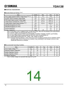
最大許容損失 vs 周囲温度
Maximum allowable dissipation vs ambient temperature
Ploss = (Pout *Rpn / Rl) *2 + Idc *Vdc
4.0
3.5
Ploss
Pout
Rpn
Rl
:Allowable Dissipation (W)
:Output Power (W)
:0.66 (Constant)
3.0
2.5
2.0
1.5
1.0
0.5
0.0
:Load Resistor (Ω)
Idc
:0.035(Constant / at VDDP=12V)
0.028(Constant / at VDDP=9V)
0.038(Constant / at VDDP=13.5V)
:Power supply voltage (V)
0
10
20
30
40
50
60
70
80
90
Vdc
周囲温度ꢀ(℃)
Ambient temperature (℃)
Maximum allowable dissipation of YDA138
YDA138 の最大許容損失
・Formula for the junction temperature
Tj = Ploss * θja + Ta
Ploss
θja
Ta
:Allowable Dissipation (W)
:35.9 (Constant/ package thermal resistance (℃/W))
:Ambient Temperature (℃)
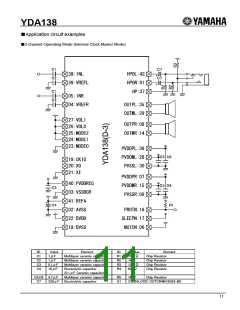
●Mounting
The package (42SSOP) for YDA138 has Thermal Pad for radiation on the bottom. This Thermal Pad does not need
soldering on the board.
・Example of Pattern
Thermal resistance of the package is 35.9℃/W. This thermal resistance was measured under the following conditions:
mounting board 136mm×85mm, copper leaf board density 154%, no wind. In addition, a part of the board that faces to
Thermal Pad is a pattern (4mm*6mm) without etching resist, the pattern is connected to the opposite side by through-hole
(φ0.4).
10

 YAMAHA [ YAMAHA CORPORATION ]