Virtex-6 FPGA Data Sheet: DC and Switching Characteristics
Speed Grade
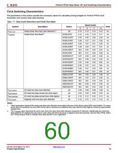
Table 73: Sample Window
Symbol
Description
Device
Units
-3
-2
-1
-1L
670
440
TSAMP
Sampling Error at Receiver Pins(1)
All
All
510
300
560
350
610
400
ps
ps
TSAMP_BUFIO
Sampling Error at Receiver Pins using BUFIO(2)
Notes:
1. This parameter indicates the total sampling error of Virtex-6 FPGA DDR input registers, measured across voltage, temperature, and
process. The characterization methodology uses the MMCM to capture the DDR input registers’ edges of operation. These measurements
include:
- CLK0 MMCM jitter
- MMCM accuracy (phase offset)
- MMCM phase shift resolution
These measurements do not include package or clock tree skew.
2. This parameter indicates the total sampling error of Virtex-6 FPGA DDR input registers, measured across voltage, temperature, and
process. The characterization methodology uses the BUFIO clock network and IODELAY to capture the DDR input registers’ edges of
operation. These measurements do not include package or clock tree skew.
Table 74: Pin-to-Pin Setup/Hold and Clock-to-Out
Speed Grade
Symbol
Description
Units
-3
Data Input Setup and Hold Times Relative to a Forwarded Clock Input Pin Using BUFIO
PSCS/TPHCS Setup/Hold of I/O clock –0.28/1.09 –0.28/1.16 –0.28/1.33 –0.18/1.79
Pin-to-Pin Clock-to-Out Using BUFIO
-2
-1
-1L
T
ns
ns
TICKOFCS
Clock-to-Out of I/O clock
4.22
4.59
5.22
5.63
Revision History
The following table shows the revision history for this document:
Date
Version
1.0
Description of Revisions
06/24/2009
07/16/2009
Initial Xilinx release.
1.1
Revised the maximum VCCAUX and VIN numbers in Table 2, page 2. Removed empty column from
Table 3, page 3. Revised specifications on Table 20, page 13. Updated Table 38, page 22 and added
notes 1 and 2. Revised TDLYCCO_RDY, TIDELAYCTRL_RPW, and TIDELAYPAT_JIT in Table 53, page 41.
Updated Table 58, page 46 to more closely match the DSP48E1 speed specifications. Updated
TTAPTCK/TTCKTAP in Table 59, page 49. Updated XC6VLX130T parameters in Table 68 through
Table 70, page 59.
08/19/2009
09/16/2009
1.2
2.0
Added values for -1L voltages and speed grade in all pertinent tables. Added VFS and notes to Table 1
and Table 2. Removed DVPPIN from the example in Figure 2. Added networking applications to
Table 41, page 25. Changed and added to the block RAM FMAX section in Table 57, page 44 including
removing Note 12. Changed FPFDMAX values and corrected units for TSTATPHAOFFSET and TOUTDUTY
in Table 64, page 52. Updated Table 71, page 60.
Added Virtex-6 HXT devices to entire document including GTH Transceiver Specifications. Updated
speed specifications as described in Switching Characteristics, includes changes in Table 51,
Table 57, Table 58, and Table 66 through Table 70. Comprehensive changes to Table 14, Table 15, and
Table 16. Added conditions to DVPPOUT and revised description of TOSKEW in Table 17. Removed VISE
specification and note from Table 18. Added note 3 to Table 23. Updated note 3 in Table 24. Updated
LVCMOS25 delays in Table 44. Updated specification for TIOTPHZ in Table 46. Removed TBUFHSKEW
from Table 71, page 60 and added values for TBUFIOSKEW. Added values in Table 74.
DS152 (v3.6) March 18, 2014
www.xilinx.com
Product Specification
62

 XILINX [ XILINX, INC ]