Virtex-6 FPGA Data Sheet: DC and Switching Characteristics
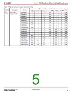
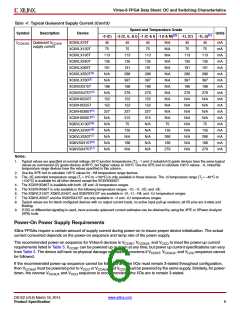
Table 4: Typical Quiescent Supply Current (Cont’d)
Speed and Temperature Grade
Units
Symbol
Description
Device
(2)
(1)
-3 (C)
45
-2 (C, E, & I) -1 (C & I) -1 (I & M)
-1L (C) -1L (I)
ICCAUXQ Quiescent VCCAUX
supply current
XC6VLX75T
45
45
N/A
N/A
N/A
N/A
N/A
N/A
N/A
N/A
N/A
N/A
N/A
N/A
N/A
75
45
45
mA
mA
mA
mA
mA
mA
mA
mA
mA
mA
mA
mA
mA
mA
mA
mA
mA
mA
XC6VLX130T
XC6VLX195T
XC6VLX240T
XC6VLX365T
XC6VLX550T(3)
XC6VLX760(3)
XC6VSX315T
XC6VSX475T(3)
XC6VHX250T
XC6VHX255T
XC6VHX380T(4)
XC6VHX565T(5)
XQ6VLX130T(6)
XQ6VLX240T(6)
XQ6VLX550T(7)
XQ6VSX315T(6)
XQ6VSX475T(7)
75
75
75
75
75
113
135
191
N/A
N/A
186
N/A
152
152
227
N/A
N/A
N/A
N/A
N/A
N/A
113
135
191
286
387
186
279
152
152
227
315
75
113
135
191
286
387
186
279
152
152
227
315
N/A
N/A
N/A
N/A
N/A
113
135
191
286
387
186
279
N/A
N/A
N/A
N/A
N/A
N/A
N/A
N/A
N/A
113
135
191
286
387
186
279
N/A
N/A
N/A
N/A
75
135
N/A
186
N/A
135
286
186
279
135
286
186
279
Notes:
1. Typical values are specified at nominal voltage, 85°C junction temperatures (T ). -1 and -2 industrial (I) grade devices have the same typical
j
values as commercial (C) grade devices at 85°C, but higher values at 100°C. Use the XPE tool to calculate 100°C values. -1L industrial
temperature range devices have the values specified in this column.
2. Use the XPE tool to calculate 125°C values for -1M temperature range devices.
3. The -2E extended temperature range (T = 0°C to +100°C) is only available in these devices. The -2I temperature range (T = –40°C to
j
j
+100°C) is available for all other devices except the XC6VHX565T.
4. The XC6VHX380T is available with both -2E and -2I temperature ranges.
5. The XC6VHX565T is only available in the following temperature ranges: -1C, -1I, -2C, and -2E.
6. The XQ6VLX130T, XQ6VLX240T, and XQ6VSX315T are available in -2I, -1I, -1M, and -1LI temperature ranges.
7. The XQ6VLX550T and the XQ6VSX475T are only available in -1I and -1LI temperature ranges.
8. Typical values are for blank configured devices with no output current loads, no active input pull-up resistors, all I/O pins are 3-state and
floating.
9. If DCI or differential signaling is used, more accurate quiescent current estimates can be obtained by using the XPE or XPower Analyzer
(XPA) tools.
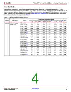
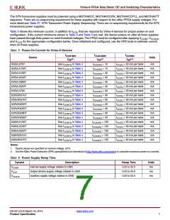
Power-On Power Supply Requirements
Xilinx FPGAs require a certain amount of supply current during power-on to insure proper device initialization. The actual
current consumed depends on the power-on sequence and ramp rate of the power supply.
The recommended power-on sequence for Virtex-6 devices is V
, V
, and V
to meet the power-up current
CCO
CCINT CCAUX
requirements listed in Table 5. V
can be powered up or down at any time, but power up current specifications can vary
CCINT
from Table 5. The device will have no physical damage or reliability concerns if V
be followed.
, V
, and V
sequence cannot
CCINT CCAUX
CCO
If the recommended power-up sequence cannot be followed and the I/Os must remain 3-stated throughout configuration,
then V must be powered prior to V or V and V must be powered by the same supply. Similarly, for power-
CCAUX
CCO
CCAUX
CCO
down, the reverse V
and V
sequence is recommended if the I/Os are to remain 3-stated.
CCAUX
CCO
DS152 (v3.6) March 18, 2014
www.xilinx.com
Product Specification
6

 XILINX [ XILINX, INC ]