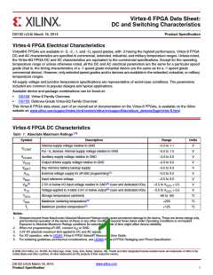
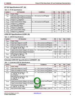
Virtex-6 FPGA Data Sheet: DC and Switching Characteristics
(1)(2)
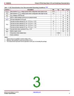
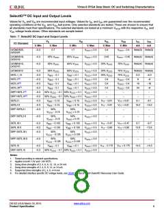
Table 3: DC Characteristics Over Recommended Operating Conditions
Symbol Description
VDRINT Data retention VCCINT voltage (below which configuration data might be lost)
Min
0.75
2.0
–
Typ
Max
–
Units
V
–
VDRI
IREF
IL
Data retention VCCAUX voltage (below which configuration data might be lost)
VREF leakage current per pin
–
–
V
–
10
10
8
µA
µA
pF
µA
µA
µA
µA
µA
nA
n
Input or output leakage current per pin (sample-tested)
Die input capacitance at the pad
–
–
(3)
CIN
–
–
Pad pull-up (when selected) @ VIN = 0V, VCCO = 2.5V
Pad pull-up (when selected) @ VIN = 0V, VCCO = 1.8V
Pad pull-up (when selected) @ VIN = 0V, VCCO = 1.5V
Pad pull-up (when selected) @ VIN = 0V, VCCO = 1.2V
Pad pull-down (when selected) @ VIN = 2.5V
Battery supply current
20
8
–
80
40
30
20
80
150
–
–
IRPU
5
–
1
–
IRPD
3
–
IBATT
–
–
1.0002
5
n
r
Temperature diode ideality factor
–
Series resistance
–
–
Ω
Notes:
1. Typical values are specified at nominal voltage, 25°C.
2. Maximum value specified for worst case process at 25°C.
3. This measurement represents the die capacitance at the pad, not including the package.
DS152 (v3.6) March 18, 2014
www.xilinx.com
Product Specification
3

 XILINX [ XILINX, INC ]