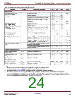
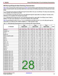
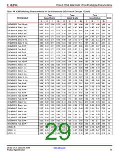
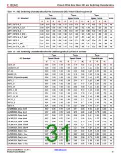
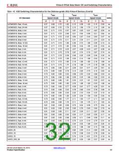
Virtex-6 FPGA Data Sheet: DC and Switching Characteristics
IOB Pad Input/Output/3-State Switching Characteristics
Table 44 (for commercial (XC) Virtex-6 devices) and Table 45 (for the Defense-grade (XQ) Virtex-6 devices) summarizes the
values of standard-specific data input delay adjustments, output delays terminating at pads (based on standard) and 3-state
delays.
T
is described as the delay from IOB pad through the input buffer to the I-pin of an IOB pad. The delay varies depending
IOPI
on the capability of the SelectIO input buffer.
T
is described as the delay from the O pin to the IOB pad through the output buffer of an IOB pad. The delay varies
IOOP
depending on the capability of the SelectIO output buffer.
T
is described as the delay from the T pin to the IOB pad through the output buffer of an IOB pad, when 3-state is
IOTP
disabled. The delay varies depending on the SelectIO capability of the output buffer.
Table 46 summarizes the value of T . T is described as the delay from the T pin to the IOB pad through the
IOTPHZ IOTPHZ
output buffer of an IOB pad, when 3-state is enabled (i.e., a high impedance state).
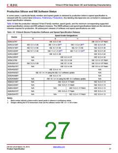
Table 44: IOB Switching Characteristics for the Commercial (XC) Virtex-6 Devices
TIOPI
TIOOP
TIOTP
I/O Standard
Speed Grade
Speed Grade
Speed Grade
Units
-3
-2
-1
-1L
-3
-2
-1
-1L
-3
-2
-1
-1L
LVDS_25
0.85 0.94 1.09 1.08 1.45 1.54 1.68 1.62 1.45 1.54 1.68 1.62
0.85 0.94 1.09 1.08 1.53 1.65 1.84 1.73 1.53 1.65 1.84 1.73
0.85 0.94 1.09 1.08 1.51 1.62 1.78 1.69 1.51 1.62 1.78 1.69
0.85 0.94 1.09 1.08 1.39 1.50 1.67 1.65 1.39 1.50 1.67 1.65
0.85 0.94 1.09 1.08 1.45 1.54 1.68 1.62 1.45 1.54 1.68 1.62
0.81 0.91 1.06 1.06 1.45 1.56 1.73 1.71 1.45 1.56 1.73 1.71
0.81 0.91 1.06 1.06 1.44 1.56 1.74 1.72 1.44 1.56 1.74 1.72
0.81 0.91 1.06 1.06 1.42 1.54 1.71 1.69 1.42 1.54 1.71 1.69
0.81 0.91 1.06 1.06 1.47 1.58 1.75 1.72 1.47 1.58 1.75 1.72
0.81 0.91 1.06 1.06 1.50 1.62 1.81 1.78 1.50 1.62 1.81 1.78
0.81 0.91 1.06 1.06 1.42 1.54 1.71 1.69 1.42 1.54 1.71 1.69
0.81 0.91 1.06 1.06 1.49 1.60 1.77 1.74 1.49 1.60 1.77 1.74
0.81 0.91 1.06 1.06 1.42 1.54 1.72 1.71 1.42 1.54 1.72 1.71
0.81 0.91 1.06 1.06 1.42 1.54 1.71 1.69 1.42 1.54 1.71 1.69
0.51 0.57 0.66 0.70 5.09 5.46 6.01 5.63 5.09 5.46 6.01 5.63
0.51 0.57 0.66 0.70 3.30 3.49 3.79 3.65 3.30 3.49 3.79 3.65
0.51 0.57 0.66 0.70 2.62 2.81 3.08 2.95 2.62 2.81 3.08 2.95
0.51 0.57 0.66 0.70 2.21 2.41 2.72 2.59 2.21 2.41 2.72 2.59
0.51 0.57 0.66 0.70 1.80 1.95 2.17 2.10 1.80 1.95 2.17 2.10
0.51 0.57 0.66 0.70 1.89 2.05 2.29 2.21 1.89 2.05 2.29 2.21
0.51 0.57 0.66 0.70 1.68 1.82 2.02 1.98 1.68 1.82 2.02 1.98
0.51 0.57 0.66 0.70 5.12 5.49 6.04 5.62 5.12 5.49 6.04 5.62
0.51 0.57 0.66 0.70 3.28 3.50 3.82 3.65 3.28 3.50 3.82 3.65
0.51 0.57 0.66 0.70 2.56 2.73 2.99 2.88 2.56 2.73 2.99 2.88
0.51 0.57 0.66 0.70 2.11 2.33 2.65 2.53 2.11 2.33 2.65 2.53
0.51 0.57 0.66 0.70 1.74 1.88 2.08 2.03 1.74 1.88 2.08 2.03
0.51 0.57 0.66 0.70 1.77 1.92 2.13 2.08 1.77 1.92 2.13 2.08
ns
ns
ns
ns
ns
ns
ns
ns
ns
ns
ns
ns
ns
ns
ns
ns
ns
ns
ns
ns
ns
ns
ns
ns
ns
ns
ns
LVDSEXT_25
HT_25
BLVDS_25
RSDS_25 (point to point)
HSTL_I
HSTL_II
HSTL_III
HSTL_I_18
HSTL_II_18
HSTL_III_18
SSTL2_I
SSTL2_II
SSTL15
LVCMOS25, Slow, 2 mA
LVCMOS25, Slow, 4 mA
LVCMOS25, Slow, 6 mA
LVCMOS25, Slow, 8 mA
LVCMOS25, Slow, 12 mA
LVCMOS25, Slow, 16 mA
LVCMOS25, Slow, 24 mA
LVCMOS25, Fast, 2 mA
LVCMOS25, Fast, 4 mA
LVCMOS25, Fast, 6 mA
LVCMOS25, Fast, 8 mA
LVCMOS25, Fast, 12 mA
LVCMOS25, Fast, 16 mA
DS152 (v3.6) March 18, 2014
www.xilinx.com
Product Specification
28

 XILINX [ XILINX, INC ]