Virtex-6 FPGA Data Sheet: DC and Switching Characteristics
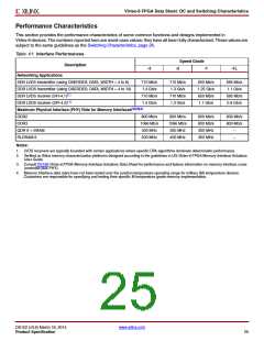
Performance Characteristics
This section provides the performance characteristics of some common functions and designs implemented in
Virtex-6 devices. The numbers reported here are worst-case values; they have all been fully characterized. These values are
subject to the same guidelines as the Switching Characteristics, page 26.
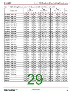
Table 41: Interface Performances
Speed Grade
Description
-3
-2
-1
-1L
Networking Applications
SDR LVDS transmitter (using OSERDES; DATA_WIDTH = 4 to 8)
DDR LVDS transmitter (using OSERDES; DATA_WIDTH = 4 to 10)
SDR LVDS receiver (SFI-4.1)(1)
710 Mb/s
1.4 Gb/s
710 Mb/s
1.4 Gb/s
710 Mb/s
1.3 Gb/s
710 Mb/s
1.3 Gb/s
650 Mb/s
1.25 Gb/s
650 Mb/s
1.1 Gb/s
585 Mb/s
1.1 Gb/s
585 Mb/s
0.9 Gb/s
DDR LVDS receiver (SPI-4.2)(1)
Maximum Physical Interface (PHY) Rate for Memory Interfaces(2)(3)(4)
DDR2
800 Mb/s
800 Mb/s
1066 Mb/s
350 MHz
400 MHz
800 Mb/s
800 Mb/s
300 MHz
350 MHz
606 Mb/s
DDR3
1066 Mb/s
400 MHz
500 MHz
800 Mb/s
QDR II + SRAM
RLDRAM II
–
–
Notes:
1. LVDS receivers are typically bounded with certain applications where specific DPA algorithms dominate deterministic performance.
2. Verified on Xilinx memory characterization platforms designed according to the guidelines in UG:Virtex-6 FPGA Memory Interface Solutions
User Guide.
3. Consult DS186:Virtex-6 FPGA Memory Interface Solutions Data Sheet for performance and feature information on memory interface cores
(controller plus PHY).
4. Memory Interface data rates have not been tested over the junction temperature operating range for military (M) temperature devices.
Customers are responsible for specifying and testing their specific M temperature grade memory implementation.
DS152 (v3.6) March 18, 2014
www.xilinx.com
Product Specification
25

 XILINX [ XILINX, INC ]