Virtex-6 FPGA Data Sheet: DC and Switching Characteristics
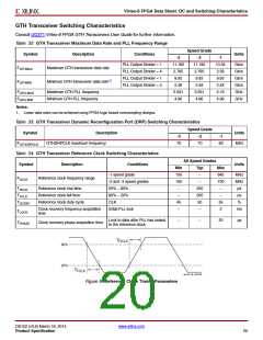
GTH Transceiver Switching Characteristics
Consult UG371:Virtex-6 FPGA GTH Transceivers User Guide for further information.
Table 32: GTH Transceiver Maximum Data Rate and PLL Frequency Range
Speed Grade
-2
Symbol
Description
Conditions
Units
-3
-1
PLL Output Divider = 1
PLL Output Divider = 4
PLL Output Divider = 1
PLL Output Divider = 4
11.182
2.795
9.92
11.182
2.795
9.92
10.32
2.58
9.92
2.48
5.16
4.96
Gb/s
Gb/s
Gb/s
Gb/s
GHz
GHz
FGTHMAX
Maximum GTH transceiver data rate
Minimum GTH transceiver data rate(1)
FGTHMIN
2.48
2.48
FGPLLMAX
FGPLLMIN
Maximum GTH PLL frequency
Minimum GTH PLL frequency
5.591
4.96
5.591
4.96
Notes:
1. Lower data rates can be achieved using FPGA logic based oversampling designs.
Table 33: GTH Transceiver Dynamic Reconfiguration Port (DRP) Switching Characteristics
Speed Grade
Symbol
Description
GTHDRPCLK maximum frequency
Units
-3
-2
-1
FGTHDRPCLK
70
70
60
MHz
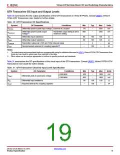
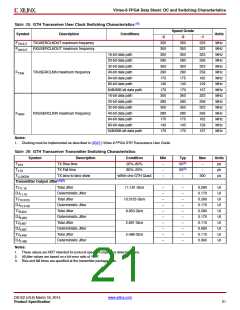
Table 34: GTH Transceiver Reference Clock Switching Characteristics
All Speed Grades
Symbol
Description
Conditions
Units
Min
150
150
–
Typ
–
Max
645
700
–
-1 speed grade
MHz
MHz
ps
FGCLK
Reference clock frequency range
-2 and -3 speed grades
20% – 80%
–
TRCLK
TFCLK
TDCREF
Reference clock rise time
Reference clock fall time
Reference clock duty cycle
200
200
50
–
80% – 20%
–
–
ps
CLK
45
–
55
2
%
Clock recovery frequency acquisition
time
Initial PLL lock
ms
TLOCK
Lock to data after PLL has locked
to the reference clock
–
–
20
µs
TPHASE
Clock recovery phase acquisition time
X-Ref Target - Figure 5
TRCLK
80%
20%
TFCLK
ds152_05_042109
Figure 5: Reference Clock Timing Parameters
DS152 (v3.6) March 18, 2014
www.xilinx.com
Product Specification
20

 XILINX [ XILINX, INC ]