Virtex-6 FPGA Data Sheet: DC and Switching Characteristics
GTH Transceiver Specifications
GTH Transceiver DC Characteristics
(1)
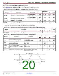
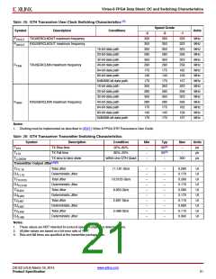
Table 25: Absolute Maximum Ratings for GTH Transceivers
Symbol
Description
Min
Max
Units
Analog supply voltage for the GTH transmitter, receiver, and common analog
circuits
–0.5
1.125
V
MGTHAVCC
MGTHAVCCRX
MGTHAVTT
Analog supply voltage for the GTH receiver circuits and common analog circuits
Analog supply voltage for the GTH transmitter termination circuits
–0.5
–0.5
–0.5
–0.5
–0.5
1.125
1.32
V
V
V
V
V
MGTHAVCCPLL Analog supply voltage for the GTH receiver and PLL circuits
1.935
1.125
1.935
VIN
Receiver (RXP/RXN) and Transmitter (TXP/TXN) absolute input voltage
Reference clock absolute input voltage
VMGTREFCLK
Notes:
1. Stresses beyond those listed under Absolute Maximum Ratings might cause permanent damage to the device. These are stress ratings only,
and functional operation of the device at these or any other conditions beyond those listed under Operating Conditions is not implied.
Exposure to Absolute Maximum Ratings conditions for extended periods of time might affect device reliability.
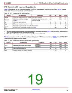
(1)(2)
Table 26: Recommended Operating Conditions for GTH Transceivers
Symbol
Description
Min
Typ
Max
Units
Analog supply voltage for the GTH transmitter, receiver, and common analog
circuits
1.075
1.1
1.125
V
MGTHAVCC
Analog supply voltage for the GTH receiver circuits and common analog
circuits
1.075
1.1
1.125
V
MGTHAVCCRX
MGTHAVTT
Analog supply voltage for the GTH transmitter termination circuits
1.140
1.710
1.2
1.8
1.26
1.89
V
V
MGTHAVCCPLL Analog supply voltage for the GTH receiver and PLL circuit
Notes:
1. Each voltage listed requires the filter circuit described in UG371:Virtex-6 FPGA GTH Transceivers User Guide.
2. Voltages are specified for the temperature range of T = –40°C to +100°C.
j
(1)(2)(3)
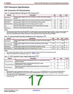
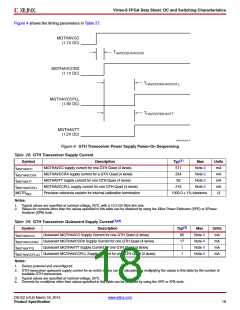
Table 27: GTH Transceiver Power Supply Sequencing
Symbol
Description
Min
Max
Units
Maximum time between powering MGTHAVCC to when MGTHAVCCRX
must be powered.
THAVCC2HAVCCRX
0
5
–
–
ms
Minimum time between powering MGTHAVCCRX to when
MGTHAVCCPLL can be powered.
THAVCCRX2HAVCCPLL
THAVCCRX2HAVTT
10
10
µs
µs
Minimum time between powering MGTHAVCCRX to when MGTHAVTT
can be powered.
Notes:
1. MGTHAVCCRX must be powered simultaneously or within T
of MGTHAVCC, but it must not precede MGTHAVCC.
HAVCC2HAVCCRX
2. MGTHAVCC and MGTHAVCCRX must be powered before MGTHAVCCPLL and MGTHAVTT. This minimum time is defined by
and T
T
.
HAVCCRX2HAVTT
HAVCCRX2HAVCCPLL
3. At any time, the condition of MGTHAVCC being present and MGTHAVCCRX not being present should not occur for more than the maximum
T
.
HAVCC2HAVCCRX
DS152 (v3.6) March 18, 2014
www.xilinx.com
Product Specification
17

 XILINX [ XILINX, INC ]