R
Pinout Descriptions
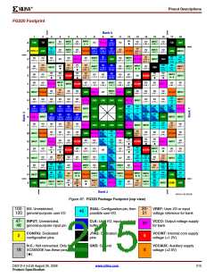
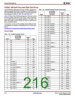
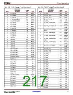
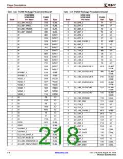
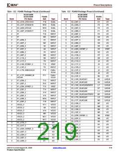
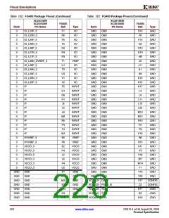
FG400: 400-ball Fine-pitch Ball Grid Array
The 400-ball fine-pitch ball grid array, FG400, supports two
different Spartan-3E FPGAs, including the XC3S1200E and
the XC3S1600E. Both devices share a common footprint for
this package as shown in Table 152 and Figure 88.
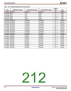
Table 152: FG400 Package Pinout (Continued)
XC3S1200E
XC3S1600E
Pin Name
FG400
Ball
Bank
0
0
0
0
0
0
0
0
0
0
0
0
0
0
0
0
0
0
0
0
0
0
0
0
0
0
0
0
0
0
0
0
0
0
0
0
0
0
0
Type
I/O
Table 152 lists all the FG400 package pins. They are sorted
by bank number and then by pin name. Pairs of pins that
form a differential I/O pair appear together in the table. The
table also shows the pin number for each pin and the pin
type, as defined earlier.
IO_L12N_0
C12
D12
E12
F12
G11
F11
E10
E11
A9
IO_L12P_0
I/O
IO_L13N_0
I/O
IO_L13P_0
I/O
IO_L15N_0/GCLK5
IO_L15P_0/GCLK4
IO_L16N_0/GCLK7
IO_L16P_0/GCLK6
IO_L18N_0/GCLK11
IO_L18P_0/GCLK10
IO_L19N_0
GCLK
GCLK
GCLK
GCLK
GCLK
GCLK
I/O
An electronic version of this package pinout table and foot-
print diagram is available for download from the Xilinx web-
site at:
http://www.xilinx.com/support/documentation/data_sheets/s3e_pin.zip
Pinout Table
A10
F9
Table 152: FG400 Package Pinout
XC3S1200E
IO_L19P_0
E9
I/O
XC3S1600E
Pin Name
FG400
Ball
Bank
0
Type
I/O
IO_L21N_0
C9
I/O
IO
IO
IO
IO
IO
IO
IO
IO
IO
IO
IO
A3
IO_L21P_0
D9
I/O
0
A8
I/O
IO_L22N_0/VREF_0
IO_L22P_0
B8
VREF
I/O
0
A12
C7
I/O
B9
0
I/O
IO_L24N_0/VREF_0
IO_L24P_0
F7
VREF
I/O
0
C10
E8
I/O
F8
0
I/O
IO_L25N_0
A6
I/O
0
E13
E16
F13
F14
G7
I/O
IO_L25P_0
A7
I/O
0
I/O
IO_L27N_0
B5
I/O
0
I/O
IO_L27P_0
B6
I/O
0
I/O
IO_L28N_0
D6
I/O
0
I/O
IO_L28P_0
C6
I/O
0
IO/VREF_0
C11
B17
C17
A18
A19
A17
A16
A15
B15
C14
D14
A13
A14
B13
C13
VREF
I/O
IO_L30N_0/VREF_0
IO_L30P_0
C5
VREF
I/O
0
IO_L01N_0
D5
0
IO_L01P_0
I/O
IO_L31N_0
A2
I/O
0
IO_L03N_0/VREF_0
IO_L03P_0
VREF
I/O
IO_L31P_0
B2
I/O
0
IO_L32N_0/HSWAP
IO_L32P_0
D4
DUAL
I/O
0
IO_L04N_0
I/O
C4
0
IO_L04P_0
I/O
IP
B18
E5
INPUT
INPUT
INPUT
INPUT
INPUT
INPUT
INPUT
INPUT
INPUT
0
IO_L06N_0
I/O
IP
0
IO_L06P_0
I/O
IP_L02N_0
C16
D16
D15
C15
E14
E15
G14
0
IO_L07N_0
I/O
IP_L02P_0
0
IO_L07P_0
I/O
IP_L05N_0
0
IO_L09N_0/VREF_0
IO_L09P_0
VREF
I/O
IP_L05P_0
0
IP_L08N_0
0
IO_L10N_0
I/O
IP_L08P_0
0
IO_L10P_0
I/O
IP_L11N_0
216
www.xilinx.com
DS312-4 (v3.8) August 26, 2009
Product Specification

 XILINX [ XILINX, INC ]