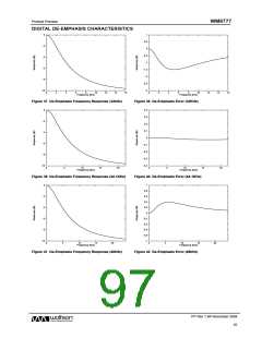
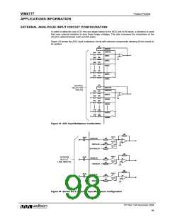
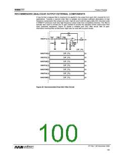
Product Preview
WM8777
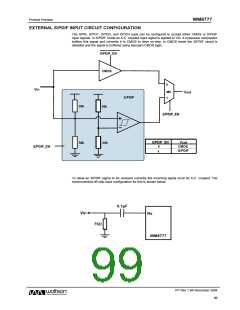
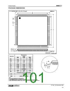
EXTERNAL S/PDIF INPUT CIRCUIT CONFIGURATION
The SPIN, GPIO1, GPIO2, and GPIO3 pads can be configured to accept either CMOS or S/PDIF
input signals. In S/PDIF mode an A.C. coupled input signal is applied to Vin. A hysteresis comparator
buffers this signal and converts it to CMOS to drive on-chip. In CMOS mode the S/PDIF circuit is
disabled and the signal is buffered using standard CMOS logic.
To allow an S/PDIF signal to be received correctly the incoming signal must be A.C. coupled. The
recommended off-chip input configuration for this is shown below:
Vin
Rx
75ꢀ
WM8777
PP Rev 1.94 November 2004
99
w

 WOLFSON [ WOLFSON MICROELECTRONICS PLC ]