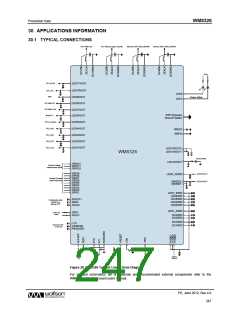
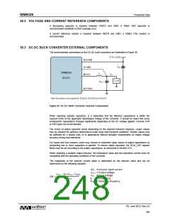
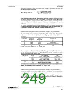
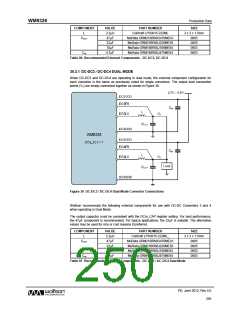
WM8326
Production Data
30.5 PCB LAYOUT
Poor PCB layout will degrade the performance and be a contributory factor in EMI, ground bounce
and resistive voltage losses. Poor regulation and instability can result.
Simple design rules can be implemented to negate these effects:
External input and output capacitors should be placed as close to the device as possible using short
wide traces between the external power components. For the DC-DC Converters, the input capacitor
placement takes priority on the DC-DC converters. (For the LDO Regulators, the placement of the
input and output capacitors have equal priority.)
Route the DC-DC converter output voltage feedback as an independent connection to the top of the
output capacitor to create a true sense of the output voltage, routing away from noisy signals such as
the LX connection.
Use a local ground island for each individual DC-DC converter connected at a single point onto a fully
flooded ground plane.
Current loop areas should be kept as small as possible with loop areas changing little during
alternating switching cycles.
PD, June 2012, Rev 4.0
252
w

 WOLFSON [ WOLFSON MICROELECTRONICS PLC ]