WM8321
Production Data
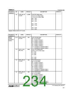
REFER TO
REGISTER
ADDRESS
BIT
LABEL
DEFAULT
DESCRIPTION
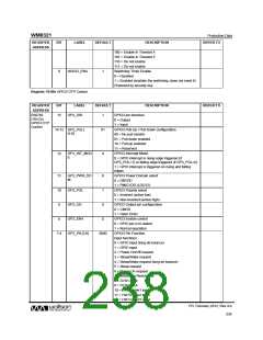
100 = Enable in Timeslot 4
101 = Enable in Timeslot 5
110 = Do not enable
111 = Do not enable
WDOG_ENA
Watchdog Timer Enable
0 = Disabled
0
1
1 = Enabled (enables the watchdog; does not reset it)
Protected by security key.
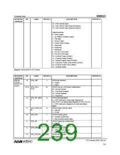
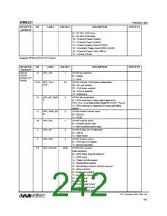
Register 781Bh GPIO2 OTP Control
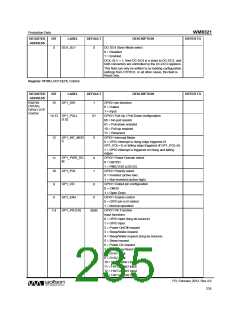
REGISTER
ADDRESS
BIT
LABEL
GP3_DIR
DEFAULT
DESCRIPTION
REFER TO
R30748
GPIO3 pin direction
0 = Output
15
1
(781Ch)
GPIO3 OTP
Control
1 = Input
GP3_PULL
[1:0]
GPIO3 Pull-Up / Pull-Down configuration
00 = No pull resistor
01 = Pull-down enabled
10 = Pull-up enabled
11 = Reserved
14:13
01
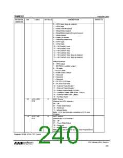
GP3_INT_MOD
E
GPIO3 Interrupt Mode
12
0
0 = GPIO interrupt is rising edge triggered (if
GP3_POL=1) or falling edge triggered (if GP3_POL=0)
1 = GPIO interrupt is triggered on rising and falling
edges
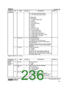
GP3_PWR_DO
M
GPIO3 Power Domain select
0 = DBVDD
11
10
9
0
1
1 = PMICVDD (LDO12)
GPIO3 Polarity select
0 = Inverted (active low)
1 = Non-Inverted (active high)
GPIO3 Output pin configuration
0 = CMOS
GP3_POL
GP3_OD
0
1 = Open Drain
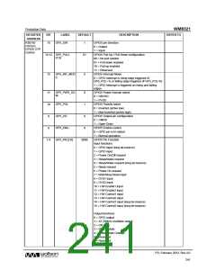
GP3_ENA
GP3_FN [3:0]
GPIO3 Enable control
0 = GPIO pin is tri-stated
1 = Normal operation
GPIO3 Pin Function
8
0
7:4
0000
Input functions:
0 = GPIO input (long de-bounce)
1 = GPIO input
2 = Power On/Off request
3 = Sleep/Wake request
4 = Sleep/Wake request (long de-bounce)
5 = Sleep request
6 = Power On request
7 = Watchdog Reset input
8 = DVS1 input
9 = DVS2 input
10 = HW Enable1 input
11 = HW Enable2 input
12 = HW Control1 input
PD, February 2012, Rev 4.0
238
w

 WOLFSON [ WOLFSON MICROELECTRONICS PLC ]