WM8321
Production Data
REFER TO
REGISTER
ADDRESS
BIT
LABEL
DEFAULT
DESCRIPTION
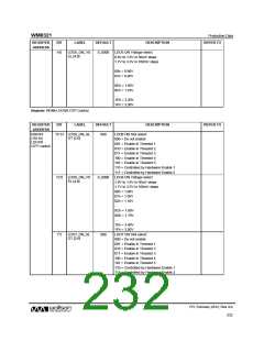
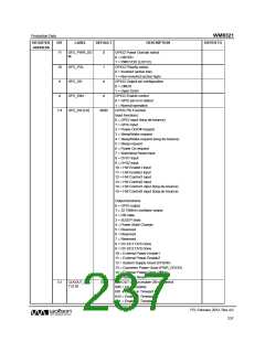
14 = HW Control1 input (long de-bounce)
15 = HW Control2 input (long de-bounce)
Output functions:
0 = GPIO output
1 = 32.768kHz oscillator output
2 = ON state
3 = SLEEP state
4 = Power State Change
5 = Reserved
6 = Reserved
7 = Reserved
8 = DC-DC1 DVS Done
9 = DC-DC2 DVS Done
10 = External Power Enable1
11 = External Power Enable2
12 = System Supply Good (SYSOK)
13 = Converter Power Good (PWR_GOOD)
14 = External Power Clock (2MHz)
15 = Auxiliary Reset
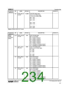
XTAL_ENA
Crystal Oscillator Enable
0 = Disabled at all times
1 = Enabled in OFF, ON, SLEEP states
2
0
(Note that the BACKUP behaviour is determined by
XTAL_BKUPENA.)
This field can only be written to by loading configuration
settings from OTP/ICE. In all other cases, this field is
Read Only.
XTAL_INH
Crystal Start-Up Inhibit
0 = Disabled
1
0
1 = Enabled
When XTAL_INH=0, the internal RC oscillator will
provide CLKOUT until the crystal oscillator is valid.
When XTAL_INH=1, the ‘ON’ transition is inhibited until
the crystal oscillator is valid.
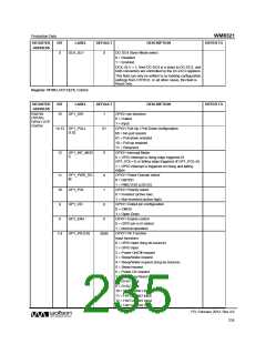
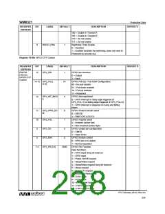
Register 781Ah GPIO1 OTP Control
REGISTER
ADDRESS
BIT
LABEL
GP2_DIR
DEFAULT
DESCRIPTION
REFER TO
R30747
(781Bh)
GPIO2 OTP
Control
GPIO2 pin direction
0 = Output
15
1
1 = Input
GP2_PULL
[1:0]
GPIO2 Pull-Up / Pull-Down configuration
00 = No pull resistor
01 = Pull-down enabled
10 = Pull-up enabled
11 = Reserved
14:13
01
GP2_INT_MOD
E
GPIO2 Interrupt Mode
12
0
0 = GPIO interrupt is rising edge triggered (if
GP2_POL=1) or falling edge triggered (if GP2_POL=0)
1 = GPIO interrupt is triggered on rising and falling
edges
PD, February 2012, Rev 4.0
236
w

 WOLFSON [ WOLFSON MICROELECTRONICS PLC ]