WFP50N06
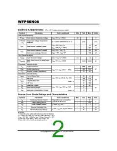
Electrical Characteristics ( TC = 25 °C unless otherwise noted )
Symbol
Parameter
Test Conditions
Min
Typ
Max
Units
Off Characteristics
BVDSS
VGS = 0V, ID = 250uA
ID = 250uA, referenced to 25 °C
Drain-Source Breakdown Voltage
60
-
-
-
-
V
Δ BVDSS
/
Breakdown Voltage Temperature
coefficient
0.07
V/°C
Δ TJ
V
DS = 60V, VGS = 0V
VDS = 48V, TC = 125 °C
GS = 20V, VDS = 0V
VGS = -20V, VDS = 0V
-
-
-
-
-
-
-
-
10
uA
uA
nA
nA
IDSS
Drain-Source Leakage Current
100
100
-100
V
Gate-Source Leakage, Forward
Gate-source Leakage, Reverse
IGSS
On Characteristics
VGS(th)
V
V
DS = VGS, ID = 250uA
GS =10 V, ID = 25.0A
Gate Threshold Voltage
2.0
-
-
4.0
V
Static Drain-Source On-state Resis-
tance
RDS(ON)
0.018
0.022
Ω
Dynamic Characteristics
Ciss
Input Capacitance
-
-
-
1050
460
70
1365
600
90
pF
Coss
Crss
Output Capacitance
VGS =0 V, VDS =25V, f = 1MHz
Reverse Transfer Capacitance
Dynamic Characteristics
td(on)
tr
td(off)
tf
Turn-on Delay Time
Rise Time
-
-
-
-
-
-
20
100
80
85
32
8
50
210
170
180
42
V
DD =30V, ID =25.0A, RG =25Ω
(Note 4, 5)
ns
Turn-off Delay Time
Fall Time
Qg
Total Gate Charge
Gate-Source Charge
VDS =48V, VGS =10V, ID =50A
(Note 4, 5)
Qgs
-
nC
Qgd
Gate-Drain Charge(Miller Charge)
-
12
-
Source-Drain Diode Ratings and Characteristics
Symbol
IS
Parameter
Test Conditions
Min.
Typ.
Max.
50
Unit.
Continuous Source Current
Pulsed Source Current
Diode Forward Voltage
Integral Reverse p-n Junction
Diode in the MOSFET
-
-
-
-
-
-
A
ISM
200
1.5
VSD
IS =50A, VGS =0V
V
trr
Reverse Recovery Time
-
-
50
70
-
-
ns
uC
IS=50A, VGS=0V, dIF/dt=100A/us
Qrr
Reverse Recovery Charge
※ NOTES
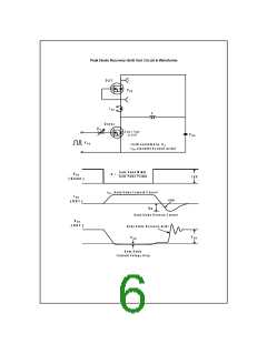
1. Repeativity rating : pulse width limited by junction temperature
2. L = 230uH, IAS =50A, VDD = 25V, RG = 25Ω , Starting TJ = 25°C
3. ISD ≤ 50A, di/dt ≤ 300A/us, VDD ≤ BVDSS, Starting TJ = 25°C
4. Pulse Test : Pulse Width ≤ 300us, Duty Cycle ≤ 2%
5. Essentially independent of operating temperature.
Copyright@Wisdom Semiconductor Inc., All rights reserved.

 WISDOM [ WISDOM TECHNOLOGIES INT`L ]