W83697HF/F
Bit 5
Bit 4
: (PIN 69 ~ 74 & 76 ~77)
= 0 GPIO 4
= 1 Fresh IF (XA!5 ~ XA10 & XA7 ~ A0)
: (PIN 66 ~ 68 & 95 ~ 97)
= 0 GPIO 5(GP52 ~ 57)
= 1 Fresh IF(XA18 ~ XA16 , ROMCS#, MEMR #, MEMW#)
Bit 0~3 : Reserved
10.5 Logical Device 0 (FDC)
CR30 (Default 0x01 if PNPCSV = 0 during POR, default 0x00 otherwise)
Bit 7 - 1 : Reserved.
Bit 0
= 1 Activates the logical device.
= 0 Logical device is inactive.
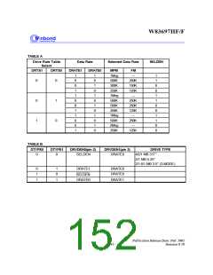
CR60, CR 61 (Default 0x03, 0xf0 if PNPCSV = 0 during POR, default 0x00, 0x00 otherwise)
These two registers select FDC I/O base address [0x100:0xFF8] on 8 byte boundary.
CR70 (Default 0x06 if PNPCSV = 0 during POR, default 0x00 otherwise)
Bit 7 - 4 : Reserved.
Bit 3 - 0 : These bits select IRQ resource for FDC.
CR74 (Default 0x02 if PNPCSV = 0 during POR, default 0x04 otherwise)
Bit 7 - 3 : Reserved.
Bit 2 - 0 : These bits select DRQ resource for FDC.
= 000
= 001
= 010
= 011
DMA0
DMA1
DMA2
DMA3
= 100 - No DMA active
111
Publication Release Date: Feb. 2002
Revision 0.70
- 140 -

 WINBOND [ WINBOND ]